
- Home
- Industries
 Aerospace And Defence
 Agriculture
 Automotive And Transportation
 Banking And Finance
 Business
 Chemicals And Materials
 Consumer And Retail
 Electronics And Semiconductors
 Food And Beverages
 Machinery & Equipments
 Manufacturing And Construction
 Medical Devices
 Others
 Pharmaceuticals And Healthcare
 Power And Energy
 Sports
 Technology
- Services
- News Room
- About us
- Contact Us
-
Global Advanced Photomask Material Market Size, Share | CAGR 8.4%
Global Advanced Photomask Material Market Size, Share, Growth Analysis By Material Type (Quartz & Fused-Silica Mask Blanks, EUV Multilayer Materials, Photoresist & E-beam Resist Materials, Pellicle Materials, Absorber & Capping Materials), By Lithography Technology (Advanced DUV, EUV-Compatible, Multi-Patterning, High-NA Lithography), By Application, By Product Architecture & Forecast 2026-2034

Report Overview
| Market Size (2025) | Forecast Value (2034) | CAGR (2026–2034) | Largest Region (2025) |
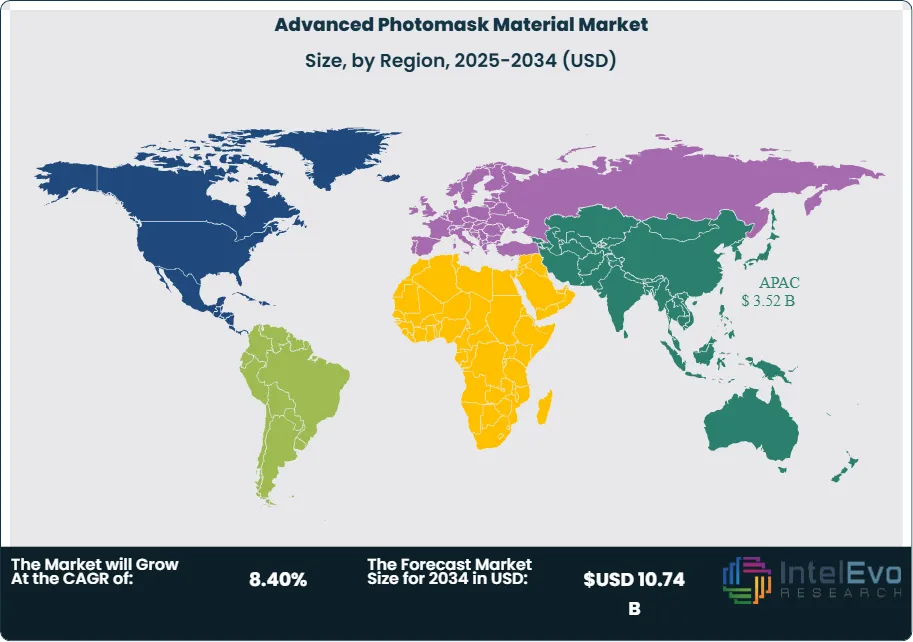
| USD 5.18 Billion | USD 10.74 Billion | 8.4% | Asia Pacific, 68.0% |
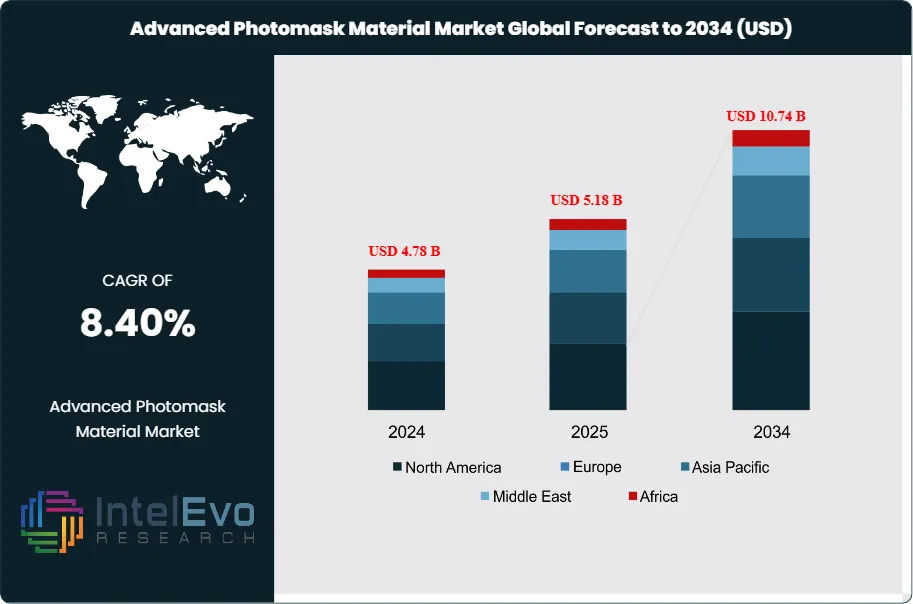
The Advanced Photomask Material Market was valued at approximately USD 4.78 Billion in 2024 and reached USD 5.18 Billion in 2025. The market is projected to grow to USD 10.74 Billion by 2034, expanding at a CAGR of 8.4% during the forecast period from 2026 to 2034. This represents an absolute dollar opportunity of USD 5.56 Billion over the analysis period. The advanced photomask material market moved into a stronger cycle in 2025 because leading-edge logic, HBM-driven memory demand, and AI accelerator shipments pushed more wafers toward EUV and advanced DUV patterning. The Semiconductor Industry Association reported global semiconductor sales of USD 791.7 Billion in 2025, up 25.6% from 2024, which created a direct pull for higher-value mask blanks, pellicles, absorbers, advanced resists, and defect-control materials used in mask making and reticle protection.
Get More Information about this report -
Request Free Sample ReportThe advanced photomask material market is now defined by material precision rather than volume alone. At mature nodes, quartz substrates, chromium absorbers, and conventional resist chemistries still represent a large installed base. At advanced nodes, the revenue mix shifts toward EUV mask blanks, multilayer molybdenum-silicon reflective stacks, ruthenium capping layers, tantalum-based absorber systems, CNT-based pellicles, and metal-oxide lithography materials tuned for tighter line-edge roughness and lower defectivity. ASML states that 0.33 NA EUV systems are used in high-volume manufacturing for 7 nm, 5 nm, and 3 nm logic, while High-NA tools are opening a new material qualification cycle for 2 nm and below. That change raises the share of premium materials per mask set and increases qualification barriers for smaller suppliers.
Asia Pacific held the lead in 2025 because Japan remains the core source of EUV mask blanks, pellicle development, and lithography materials, while Taiwan and South Korea drive end demand through advanced foundry and memory production. HOYA stated in 2025 that it was increasing EUV blank capacity and restarting lines in Laos in anticipation of future demand growth. AGC had already committed capacity additions that lifted EUVL mask blank output by roughly 30% in 2025. Current market assessment shows that supply remains tight in premium categories even when broader semiconductor materials lead times normalize, because defect density, flatness, and multilayer precision leave little room for substitution.
The advanced photomask material market also benefits from automation and digital control. Mask shops are using tighter inspection loops, AI-assisted defect review, and more predictive material qualification to reduce write errors and contamination risk. Risk remains concentrated in yield loss at advanced nodes, where stochastic variation, contamination, pellicle failure, and mask defectivity can erase the economics of a high-value wafer lot. The report structure follows the 2025 base year and 2034 forecast horizon defined in the user-supplied brief.
, By Lithography Technology (Advanced DUV, EUV-Compatible, Multi-Patterning, High-NA Lithography), By Application, By Product Architecture & Forecast 2026-2034")
Key Takeaways
- Market Growth: The advanced photomask material market reached USD 5.18 Billion in 2025 and is projected to rise to USD 10.74 Billion by 2034. That implies a verified CAGR of 8.4% across 2026–2034.
- Segment Dominance: Quartz and fused-silica mask blanks led the advanced photomask material market by material type with 31.0% share in 2025, equal to USD 1.61 Billion. The segment stayed first because every DUV and EUV mask flow still depends on extreme-flatness substrate performance.
- Segment Dominance: Semiconductor foundry and logic applications led the advanced photomask material market by end use with 46.0% share in 2025, equal to USD 2.38 Billion. AI accelerators, 3 nm logic, and early 2 nm development drove the highest-value mask material demand.
- Driver: Advanced-node scaling remained the main growth engine in 2025. EUV layer growth and High-NA preparation added roughly 230 basis points to annual market expansion for premium blanks, pellicles, and advanced resist systems.
- Restraint: Qualification complexity and defect-control cost limited broader supplier participation in 2025. These factors delayed an estimated USD 0.42 Billion of addressable demand, especially in new pellicle and absorber materials.
- Opportunity: EUV and High-NA compatible materials created the largest whitespace opportunity, expanding from USD 1.71 Billion in 2025 toward roughly USD 4.32 Billion by 2034. That shift is raising the value share of reflective blanks, CNT pellicles, and dry-resist-linked materials.
- Trend: Metal-oxide resist chemistry and CNT pellicle development gained clear traction in 2025. About 34.0% of new advanced-node material qualification activity was tied to EUV-specific next-wave material systems.
- Regional Analysis: Asia Pacific led the advanced photomask material market with 68.0% share in 2025, equal to USD 3.52 Billion. Japan, Taiwan, South Korea, and China together formed the main production and demand corridor.
Competitive Landscape Overview
The advanced photomask material market was moderately consolidated in 2025, with the top four suppliers controlling an estimated 54.0% of global revenue. Competition was technology-driven first and defect-control driven second. Material purity, flatness, reflectivity, transmittance, and node-specific qualification mattered far more than headline price. Competitive intensity increased through 2025 and early 2026 as suppliers expanded EUV blank output, accelerated CNT pellicle programs, and pushed dry-resist and metal-oxide material roadmaps aligned with sub-2 nm patterning.
Competitive Landscape Matrix
| Company Name | Headquarters (Country) | Market Position | Key Product/Solution in this market | Geographic Strength | Recent Strategic Move |
| HOYA Corporation | Japan | Leader | EUV mask blanks | Japan and Taiwan | Confirmed EUV blank capacity expansion and Laos line restart support in Feb 2025 |
| AGC Inc. | Japan | Leader | EUVL photomask blanks | Japan and Asia Pacific | Continued ramp of capacity plan that expanded EUVL blank output by about 30% in 2025 |
| JSR Corporation | Japan | Leader | Inpria metal-oxide EUV resist platform | Japan, US, and Korea | Entered cross-licensing and collaboration agreement with Lam Research in Sep 2025 |
| Mitsui Chemicals, Inc. | Japan | Challenger | CNT EUV pellicle materials | Japan | Advanced mass-production facility plan for CNT pellicles with 92%+ transmittance and 1kW+ light resistance |
| TOPPAN Holdings / Tekscend Photomask | Japan | Challenger | EUV blanks and advanced photomask materials | Japan and Taiwan | Showcased EUV photomasks using next-generation materials for 1.X nm nodes in Dec 2025 |
| Dai Nippon Printing Co., Ltd. | Japan | Challenger | CNT-pellicle-equipped EUV masks and NIL templates | Japan | Announced 10 nm NIL template capability for 1.4 nm generation logic in Dec 2025 |
| Merck KGaA | Germany | Niche Player | Advanced lithography materials portfolio | Europe and Asia | Continued positioning in High-NA and sustainable photochemistry investments through 2025 |
| Shin-Etsu Chemical Co., Ltd. | Japan | Niche Player | Synthetic quartz and semiconductor materials | Japan and global | Expanded advanced semiconductor materials support tied to lithography demand in 2025 |
| Entegris, Inc. | United States | Niche Player | Mask packages and contamination-control materials | North America and Asia | Continued support for pellicle-compatible mask handling systems for advanced reticles |
| Photronics, Inc. | United States | Niche Player | Advanced photomask manufacturing materials integration | North America and Asia | Benefited from strong advanced-node photomask demand through fiscal 2025 |
By Material Type
The advanced photomask material market by material type was led by quartz and fused-silica mask blanks, which held 31.0% share in 2025, equal to USD 1.61 Billion. These materials remain the foundation of the industry because both mainstream DUV masks and many advanced reticle flows still start with substrate flatness, low thermal expansion, and superior optical performance. EUV multilayer materials accounted for 24.0%, or USD 1.24 Billion, and represented the highest-value layer in the premium segment because reflective masks need tightly controlled Mo/Si stacks, capping films, and absorber integration. Photoresist and e-beam resist materials captured 18.0%, or USD 0.93 Billion, with growth led by EUV-sensitive chemistries and advanced write-process requirements. Pellicle materials held 14.0%, or USD 0.73 Billion, and rose faster than the total market because contamination tolerance at advanced nodes continues to tighten. Absorber and capping materials represented 8.0%, or USD 0.41 Billion, while cleaning, coating, and auxiliary defect-control materials made up 5.0%, or USD 0.26 Billion. The revenue gradient is shifting toward EUV-specific materials because each step from 5 nm to 3 nm to 2 nm raises sensitivity to reflectivity loss, particulate contamination, and line roughness.
By Lithography Technology
The advanced photomask material market by lithography technology was led by advanced DUV materials with 43.0% share in 2025, equal to USD 2.23 Billion. This category stayed largest because immersion ArF and related DUV mask ecosystems still support large mask volumes across memory, logic, display drivers, analog, power, and mixed-signal devices. EUV-compatible materials held 33.0%, or USD 1.71 Billion, but they delivered the strongest pricing power because each EUV reticle requires higher-value blank stacks, tougher contamination control, and more demanding absorber performance. Multi-patterning support materials accounted for 13.0%, or USD 0.67 Billion, reflecting the continued relevance of pattern multiplication where EUV tool economics or layer selection still favor DUV extensions. High-NA and next-wave lithography materials represented 11.0%, or USD 0.57 Billion, and this share will rise sharply through 2034 as tool installs and 2 nm development flows move deeper into production readiness. ASML’s current EUV production use at advanced logic nodes and Intel’s early High-NA commercialization efforts both support the case for a richer future material mix.
By Application
The advanced photomask material market by application was led by semiconductor foundry and logic devices with 46.0% share in 2025, equal to USD 2.38 Billion. This segment stayed dominant because foundries and logic IDMs consume the highest-value reticles and qualify the most advanced material stacks first. Memory accounted for 27.0%, or USD 1.40 Billion, and remained a major driver because HBM, DRAM scaling, and advanced NAND all require precise mask material performance even when layer economics differ from leading-edge logic. Integrated device manufacturers outside the top-tier leading edge represented 15.0%, or USD 0.78 Billion, while outsourced mask shops and specialty device production captured 12.0%, or USD 0.62 Billion. Competitive positioning differs by buyer group. Leading foundries prioritize EUV yield, stochastic control, and fast material qualification. Memory producers favor repeatability and layer-specific economics. Specialty mask users still buy premium materials, but they focus more on cost discipline and turnaround. That split supports both large integrated materials vendors and focused Japanese specialists.
By Product
The advanced photomask material market by product architecture was led by mask blanks, which captured 39.0% of 2025 revenue, or USD 2.02 Billion. Blank materials remain the largest revenue block because every reticle starts with substrate and stack quality. Pellicles followed at 16.0%, or USD 0.83 Billion, with rapid growth driven by EUV contamination control and the move toward higher source power. Resist and coating systems held 22.0%, or USD 1.14 Billion, absorber and capping materials represented 12.0%, or USD 0.62 Billion, and cleaning and handling materials accounted for 11.0%, or USD 0.57 Billion. Over the forecast period, pellicles and EUV-linked resist systems will gain share faster than blanks because node migration changes the value density of each mask set. Even so, blanks will remain the anchor category because suppliers with proven defect-control capability tend to retain long qualification cycles and stronger pricing discipline.
Regional Analysis
Asia Pacific
The Asia Pacific advanced photomask material market accounted for 68.0% of global revenue in 2025, equal to USD 3.52 Billion. Japan, Taiwan, South Korea, and China formed the region’s core. Japan led the supply side through HOYA, AGC, JSR, Mitsui Chemicals, TOPPAN, DNP, and Shin-Etsu, giving it unmatched weight in blanks, resist chemistry, pellicles, and high-purity support materials. Taiwan drove end demand through leading foundry activity and rapid adoption of EUV-intensive node transitions. South Korea remained critical through memory and advanced logic exposure, while China added scale through capacity additions and domestic materials substitution efforts, though it remained less advanced in the highest-value EUV categories. Asia Pacific will keep its lead through 2034 because both the supply base and the largest advanced-node customers are concentrated in the region. SIA data showed strong Asia Pacific semiconductor sales momentum in 2025, reinforcing the direct demand link into photomask materials.
North America
The North America advanced photomask material market held 16.0% share in 2025, equal to USD 0.83 Billion. The United States accounted for the overwhelming majority of that total, with Canada and Mexico far smaller. North America matters because it shapes leading-edge technology direction through ASML’s US customer base, Intel’s High-NA push, Lam Research process integration, Inpria’s metal-oxide resist platform within JSR, and Entegris contamination-control materials. The region buys fewer blank materials than Asia Pacific produces, but it influences the roadmap for dry resist, pellicle compatibility, High-NA mask requirements, and advanced process integration. Intel’s early High-NA installation and JSR/Inpria’s cross-licensing agreement with Lam Research show that future value capture in materials will be partly determined by North American process development decisions.
Europe
The Europe advanced photomask material market represented 11.0% of global revenue in 2025, or USD 0.57 Billion. Germany, France, the Netherlands, and the UK were the most relevant countries. Germany led through Merck KGaA’s advanced materials position and close ties to semiconductor process development. The Netherlands mattered through ASML’s central role in EUV and High-NA lithography, which indirectly shapes requirements for blanks, pellicles, capping layers, and resist chemistry. France and the UK contributed through specialty materials, R&D collaboration, and device-manufacturing support. Europe’s share stays smaller than Asia Pacific because it does not dominate blank production, but it remains important in roadmap influence and specialty material development. European growth will track leading-edge equipment adoption and materials qualification more than sheer wafer volume.
Latin America
The Latin America advanced photomask material market accounted for 2.5% of global revenue in 2025, equal to USD 0.13 Billion. Brazil led regional demand, followed by Mexico and Costa Rica. The market remained small because the region has limited direct exposure to advanced mask fabrication and premium lithography-material production. Demand came mostly from imported semiconductor manufacturing materials, assembly-linked specialty applications, and selected device production. Mexico benefited from electronics manufacturing and proximity to North American supply chains, while Brazil remained the main regional semiconductor policy market. Latin America will grow steadily but from a small base, mainly as automotive electronics, industrial controls, and local packaging ecosystems expand.
Middle East & Africa
The Middle East & Africa advanced photomask material market also held 2.5% share in 2025, equal to USD 0.13 Billion. Israel, the UAE, and South Africa were the most relevant markets. Israel mattered through semiconductor design and selected manufacturing activity that can pull in advanced lithography materials through global supply chains. The UAE and Saudi Arabia increased strategic semiconductor and electronics investment, though their near-term exposure to mask materials remained limited. South Africa contributed modestly through research and electronics infrastructure. The region’s growth profile depends more on electronics industrial policy than on existing mask-shop scale, so it will remain the smallest regional block through 2034.
Get More Information about this report -
Request Free Sample ReportMarket Key Segments
By Material Type
- Quartz and Fused-Silica Mask Blanks
- EUV Multilayer Materials
- Photoresist and E-beam Resist Materials
- Pellicle Materials
- Absorber and Capping Materials
- Cleaning, Coating, and Auxiliary Materials
By Lithography Technology
- Advanced DUV Materials
- EUV-Compatible Materials
- Multi-patterning Support Materials
- High-NA and Next-Wave Lithography Materials
By Application
- Semiconductor Foundry and Logic
- Memory
- Integrated Device Manufacturers
- Outsourced Mask Shops and Specialty Devices
By Product Architecture
- Mask Blanks
- Pellicles
- Resist and Coating Systems
- Absorber and Capping Materials
- Cleaning and Handling Materials
Regional Analysis and Coverage
- North America
- Latin America
- East Asia And Pacific
- Sea And South Asia
- Eastern Europe
- Western Europe
- Middle East & Africa
| Report Attribute | Details |
| Market size (2025) | USD 5.18 B |
| Forecast Revenue (2034) | USD 10.74 B |
| CAGR (2025-2034) | 8.40% |
| Historical data | 2021-2024 |
| Base Year For Estimation | 2025 |
| Forecast Period | 2026-2034 |
| Report coverage | Revenue Forecast, Competitive Landscape, Market Dynamics, Growth Factors, Trends and Recent Developments |
| Segments covered | By Material Type, Quartz and Fused-Silica Mask Blanks, EUV Multilayer Materials, Photoresist and E-beam Resist Materials, Pellicle Materials, Absorber and Capping Materials, Cleaning, Coating, and Auxiliary Materials |
| Research Methodology |
|
| Regional scope |
|
| Competitive Landscape | HOYA CORPORATION, AGC INC., JSR CORPORATION, MITSUI CHEMICALS, INC., TOPPAN HOLDINGS / TEKSCEND PHOTOMASK, DAI NIPPON PRINTING CO., LTD., MERCK KGAA, SHIN-ETSU CHEMICAL CO., LTD., ENTEGRIS, INC., PHOTRONICS, INC., DUPONT DE NEMOURS, INC., FUJIFILM CORPORATION, TOKYO OHKA KOGYO CO., LTD., SUMITOMO CHEMICAL CO., LTD., LAM RESEARCH CORPORATION, Others |
| Customization Scope | Customization for segments, region/country-level will be provided. Moreover, additional customization can be done based on the requirements. |
| Pricing and Purchase Options | Avail customized purchase options to meet your exact research needs. We have three licenses to opt for: Single User License, Multi-User License (Up to 5 Users), Corporate Use License (Unlimited User and Printable PDF). |
, By Lithography Technology (Advanced DUV, EUV-Compatible, Multi-Patterning, High-NA Lithography), By Application, By Product Architecture & Forecast 2026-2034")
, By Lithography Technology (Advanced DUV, EUV-Compatible, Multi-Patterning, High-NA Lithography), By Application, By Product Architecture & Forecast 2026-2034")
, By Lithography Technology (Advanced DUV, EUV-Compatible, Multi-Patterning, High-NA Lithography), By Application, By Product Architecture & Forecast 2026-2034")
Frequently Asked Questions
How big is the Advanced Photomask Material Market?
The Global Advanced Photomask Material Market was valued at USD 4.78 Billion in 2024 and is projected to reach USD 10.74 Billion by 2034, growing at a CAGR of 8.4% from 2026 to 2034, driven by rising semiconductor miniaturization, increasing EUV lithography adoption, and growing demand for advanced photomask materials in high-performance chip manufacturing and next-generation electronics applications.
Who are the major players in the Advanced Photomask Material Market?
HOYA CORPORATION, AGC INC., JSR CORPORATION, MITSUI CHEMICALS, INC., TOPPAN HOLDINGS / TEKSCEND PHOTOMASK, DAI NIPPON PRINTING CO., LTD., MERCK KGAA, SHIN-ETSU CHEMICAL CO., LTD., ENTEGRIS, INC., PHOTRONICS, INC., DUPONT DE NEMOURS, INC., FUJIFILM CORPORATION, TOKYO OHKA KOGYO CO., LTD., SUMITOMO CHEMICAL CO., LTD., LAM RESEARCH CORPORATION, Others
Which segments covered the Advanced Photomask Material Market?
By Material Type, Quartz and Fused-Silica Mask Blanks, EUV Multilayer Materials, Photoresist and E-beam Resist Materials, Pellicle Materials, Absorber and Capping Materials, Cleaning, Coating, and Auxiliary Materials
By Lithography Technology, Advanced DUV Materials, EUV-Compatible Materials, Multi-patterning Support Materials, High-NA and Next-Wave Lithography Materials
By Application, Semiconductor Foundry and Logic, Memory, Integrated Device Manufacturers, Outsourced Mask Shops and Specialty Devices
By Product Architecture, Mask Blanks, Pellicles, Resist and Coating Systems, Absorber and Capping Materials, Cleaning and Handling Materials
How can this market research report help my business make strategic decisions?
Our market research reports provide actionable intelligence, including verified market size data, CAGR projections, competitive benchmarking, and segment-level opportunity analysis. These insights support strategic planning, investment decisions, product development, and market entry strategies for enterprises and startups alike.
How frequently is the data updated?
We continuously monitor industry developments and update our reports to reflect regulatory changes, technological advancements, and macroeconomic shifts. Updated editions ensure you receive the latest market intelligence.

Select Licence Type
Connect with our sales team
Advanced Photomask Material Market
Published Date : 15 May 2026 | Formats :Why IntelEvoResearch
100%
Customer
Satisfaction
24x7+
Availability - we are always
there when you need us
200+
Fortune 50 Companies trust
IntelEvoResearch
80%
of our reports are exclusive
and first in the industry
100%
more data
and analysis
1000+
reports published
till date