
- Home
- Industries
 Aerospace And Defence
 Agriculture
 Automotive And Transportation
 Banking And Finance
 Business
 Chemicals And Materials
 Consumer And Retail
 Electronics And Semiconductors
 Food And Beverages
 Machinery & Equipments
 Manufacturing And Construction
 Medical Devices
 Others
 Pharmaceuticals And Healthcare
 Power And Energy
 Sports
 Technology
- Services
- News Room
- About us
- Contact Us
-
Global Chiplet Architecture Market Size, Share & Forecast | CAGR 20.3%
Global Chiplet Architecture Market Size, Share Analysis By Type (Compute, Memory, I/O, AI/ML Accelerator, GPU, Network), By Packaging (2.5D, 3D, FOWLP, EMIB, TSV, Hybrid Bonding), By Application (HPC, AI/ML, Data Centers, Consumer Electronics, Automotive, 5G Infrastructure), By End-Use, By Interconnect Protocol Region & Key Players-Industry Segment Overview, Market Dynamics, Competitive Strategies, Trends & Forecast 2026-2034

Report Overview
| Market Size (2025) | Forecast Value (2034) | CAGR (2026-2034) | Largest Region (2025) |
|---|---|---|---|
| USD 12.3 Billion | USD 65.0 Billion | 20.3% | North America, 36.0% |
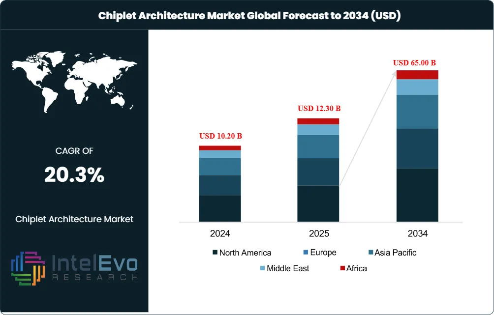
The Chiplet Architecture Market was valued at USD 10.20 Billion in 2024 and USD 12.30 Billion in 2025. The market is projected to reach USD 65.00 Billion by 2034, expanding at a CAGR of 20.3% during the forecast period from 2026 to 2034. This represents an absolute dollar opportunity of USD 52.7 Billion over the analysis period, more than five times the 2025 base. The Chiplet Architecture Market is being driven by the structural transition from monolithic system-on-chip design to modular, heterogeneous integration that combines specialized dies fabricated on different process nodes inside a single advanced package, anchored by AI accelerator demand, hyperscaler infrastructure scale-out, and the physical limits of reticle-size monolithic silicon.
Get More Information about this report -
Request Free Sample ReportThree structural drivers anchor Chiplet Architecture Market expansion through 2034. First, the UCIe Consortium released the UCIe 3.0 specification on 5 August 2025 doubling per-lane data rates to 48 GT/s and 64 GT/s, with the consortium now exceeding 140 members including AMD, Arm, ASE, Google Cloud, Intel, Meta, Microsoft, Qualcomm, Samsung, TSMC, NVIDIA, and Alibaba. Second, AMD's Instinct MI300X chiplet-based GPU integrating CPU, GPU, and HBM3 dies in a 3D package anchored AMD's transition into AI infrastructure leadership, with AMD Q4 2025 earnings showing GPU revenue exceeding CPU revenue per AnandTech reporting. Third, SK Hynix began HBM4 mass production in H2 2025 with 2026 capacity sold out by H1 2025, delivering more than 1.65 TB/s bandwidth per stack at 30% lower power than HBM3E and tightly coupling memory chiplet evolution to packaging roadmaps.
Patent filings in chiplet interconnect grew from 152 in 2017 to 1,070 in 2024, a seven-fold increase, with 2022-2024 alone accounting for 55% of historical patent activity per PatSnap analysis. UCIe 3.0 introduced support for 48 GT/s and 64 GT/s on UCIe-S 2D Standard Package and UCIe-A 2.5D Advanced Package designs, with full backward compatibility to UCIe 1.0 and 1.1. Optical I/O chiplets are emerging, with Ayar Labs' TeraPHY optical engine delivering 8 Tbps of bandwidth as the first UCIe-compliant optical interconnect chiplet. TSMC's CoWoS, Intel's EMIB, and Samsung's I-Cube advanced packaging platforms are scaling to support multi-reticle-size composite dies for hyperscaler AI accelerators.
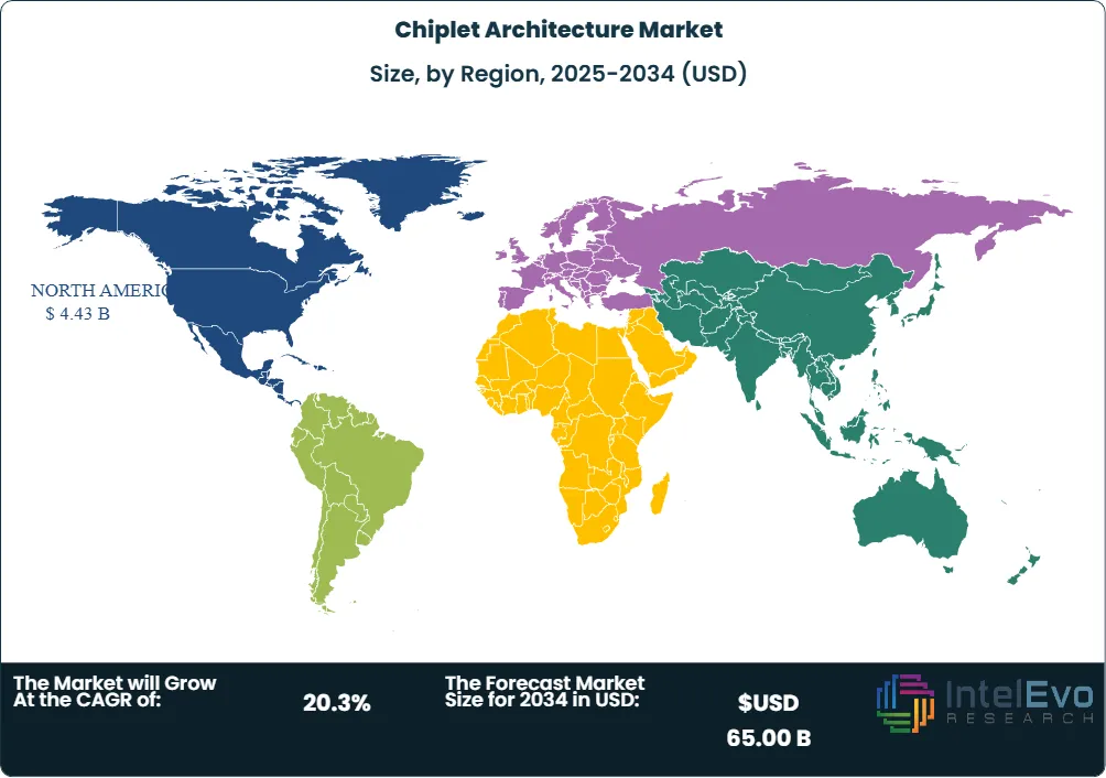
North America led the Chiplet Architecture Market with 36.0% revenue share in 2025, anchored by AMD (Santa Clara), Intel Corporation (Santa Clara), NVIDIA Corporation (Santa Clara), Marvell Technology (Santa Clara), and Broadcom Inc. (Palo Alto). Asia Pacific is the largest manufacturing region with 30.0% share concentrated in Taiwan (TSMC, ASE), South Korea (Samsung Electronics, SK Hynix), and Japan (Renesas, Sony Semiconductor), and is the fastest-growing region at over 24% CAGR through 2034. Europe holds 27.0% share led by Germany, the Netherlands (ASML), and the United Kingdom (Arm). The forward outlook through 2034 favors UCIe-compliant 2.5D and 3D heterogeneous integration combining HBM4, GPU compute dies, CPU dies, optical I/O, and specialized accelerators inside multi-die System-in-Package (SiP) architectures.
Market Definition & Scope
The Chiplet Architecture Market is defined as the design, manufacture, packaging, and integration of modular semiconductor dies (chiplets) combined within a single package to deliver heterogeneous integrated circuits with performance, scalability, and cost characteristics that monolithic system-on-chip designs cannot achieve. The market encompasses processor chiplets (CPU, GPU, AI accelerator, FPGA), memory chiplets (HBM3, HBM3E, HBM4), I/O chiplets (electrical and optical), interconnect IP (UCIe, BoW, AIB), and the advanced packaging substrate technologies (2.5D silicon interposer, EMIB, CoWoS, I-Cube, fan-out wafer-level packaging, 3D hybrid bonding) that integrate them.
This analysis includes branded chiplet-based products such as AMD EPYC and Instinct, Intel Ponte Vecchio and Granite Rapids, NVIDIA Blackwell, Apple M-series, and TSMC InFO and CoWoS platforms. The scope explicitly excludes traditional monolithic SoCs without chiplet integration, basic multi-chip modules without standardized die-to-die interconnect, and discrete component co-packaging unrelated to high-bandwidth interconnect protocols. The Chiplet Architecture Market sits within the broader semiconductor and advanced packaging category, accounting for an estimated 15-18% of total semiconductor advanced packaging spend in 2025 and rising rapidly toward 25-30% by 2030.
, By Packaging (2.5D, 3D, FOWLP, EMIB, TSV, Hybrid Bonding), By Application (HPC, AI/ML, Data Centers, Consumer Electronics, Automotive, 5G Infrastructure), By End-Use, By Interconnect Protocol Region & Key Players-Industry Segment Overview, Market Dynamics, Competitive Strategies, Trends & Forecast 2026-2034")
Key Takeaways
- Market Growth: The Chiplet Architecture Market grows from USD 12.3 Billion in 2025 to USD 65.0 Billion by 2034 at a CAGR of 20.3%, generating USD 52.7 Billion in absolute new revenue.
- Segment Dominance: CPU and GPU compute chiplets captured approximately 47.0% of the Chiplet Architecture Market in 2025, equivalent to USD 5.78 Billion, anchored by AMD EPYC, Instinct MI300X, Intel Granite Rapids, and NVIDIA Blackwell architectures.
- Segment Dominance: 2.5D and 3D advanced packaging held approximately 35.3% share of chiplet revenue in 2025 per Coherent Market Insights, equivalent to USD 4.34 Billion, with TSMC CoWoS, Intel EMIB, and Samsung I-Cube anchoring delivery capacity.
- Driver: The UCIe Consortium released UCIe 3.0 specification on 5 August 2025 supporting 48 GT/s and 64 GT/s data rates, while membership exceeds 140 companies including AMD, Intel, TSMC, Samsung, NVIDIA, Microsoft, Google, Meta, Qualcomm, Arm, and Alibaba.
- Restraint: Thermal management challenges arising from concentrated heat sources, supply chain concentration in TSMC CoWoS capacity (sold out through 2026), and high initial costs for advanced packaging infrastructure constrain near-term scaling.
- Opportunity: Optical I/O chiplets represent a USD 6 Billion forecast opportunity by 2034, illustrated by Ayar Labs' TeraPHY 8 Tbps UCIe-compliant optical interconnect chiplet and the consortium's 2026-2028 deployment timeline for co-packaged optics.
- Trend: HBM4 mass production began in H2 2025 with SK Hynix delivering 1.65 TB/s per stack at 30% lower power than HBM3E, while SK Hynix's entire 2026 HBM volume sold out by H1 2025 per Korea Economic Daily reporting.
- Regional: North America held 36.0% Chiplet Architecture Market share in 2025 at USD 4.43 Billion, with the United States contributing approximately USD 4.10 Billion or roughly 93% of the regional total.
Key Insights Summary
- The UCIe Consortium released UCIe 3.0 specification on 5 August 2025 in Beaverton, Oregon, doubling per-lane data rates to 48 GT/s and 64 GT/s on UCIe-S 2D Standard Package and UCIe-A 2.5D Advanced Package designs while preserving full backward compatibility with UCIe 1.0 and 1.1.
- UCIe Consortium membership exceeded 140 companies in 2025 per The Next Platform reporting, with board members AMD, Arm, ASE Group, Google Cloud, Intel Corporation, Meta, Microsoft, Qualcomm, Samsung, TSMC, plus Alibaba and NVIDIA elected in August 2022.
- SK Hynix leads the HBM market with 62% share as of Q2 2025 per PatSnap, followed by Micron at 21% and Samsung at 17%, with SK Hynix's entire 2026 HBM volume sold out by H1 2025 and HBM4 mass production beginning H2 2025.
- AMD reported Q4 2025 earnings showing GPU revenue exceeding CPU revenue for the first time in a quarter per The Next Platform reporting on 4 February 2026, driven by the chiplet-based Instinct MI300X 3D architecture combining CPU, GPU, and HBM dies in one package.
- Patent filings in chiplet interconnect grew from 152 in 2017 to 1,070 in 2024 (a seven-fold increase) per PatSnap, with the period from 2022 to 2024 alone accounting for 55% of all historical patent activity in the domain across 5,535 filings.
- Ayar Labs raised a strategic round in 2025 led by Neuberger Berman with participation from ARK Invest, Insight Partners, Qatar Investment Authority, Sequoia Global Equities, AMD, Alchip, MediaTek, and NVIDIA to scale TeraPHY optical I/O chiplets compliant with UCIe.
- The CHIPS and Science Act of 2022 funded over USD 52.7 Billion in US semiconductor investments, anchoring TSMC Arizona, Intel Ohio, Samsung Texas, and Micron New York fabs that will produce chiplet-based devices through 2030.
Competitive Landscape Overview
The Chiplet Architecture Market is moderately consolidated, with the top four vendors Intel Corporation, AMD (Advanced Micro Devices), TSMC (Taiwan Semiconductor Manufacturing Company), and NVIDIA Corporation estimated to hold a combined 55-62% share of disclosed Chiplet Architecture Market revenue in 2025. Competition spans three patterns: vertically integrated chiplet designers and manufacturers (Intel, Samsung), fabless designers leveraging foundry chiplet capacity (AMD, NVIDIA, Qualcomm, Marvell, Broadcom, Apple), and pure-play foundry and OSAT (Outsourced Semiconductor Assembly and Test) providers (TSMC, ASE, Amkor, JCET).
Competitive evolution is moving toward open standards interoperability via UCIe 3.0, dense memory integration via HBM4, and optical I/O chiplet adoption. AMD Instinct MI300X integrates CPU, GPU, and HBM3 dies via a 3D chiplet architecture launched in late 2023, with successor MI350 and MI400 series advancing through 2026. Intel Ponte Vecchio packs 47 chiplets in a single package per Data Center Dynamics reporting, while Granite Rapids and Falcon Shores extend Intel's chiplet roadmap. Specialist challengers Marvell, Broadcom, Astera Labs, Alchip, MediaTek, Renesas, Sony Semiconductor, NHanced Semiconductors, and Ayar Labs occupy strong positions in custom-silicon, networking, and optical I/O.
The competitive matrix below summarizes leading players in the Chiplet Architecture Market, their headquarters, market position, primary product offering, geographic strength, and the most recent strategic move verified through public disclosures during the trailing 18 months.
Competitive Landscape Matrix
| Company | HQ Country | Position | Key Product | Geographic Strength | Recent Strategic Move (Trailing 18 Months) |
|---|---|---|---|---|---|
| Intel Corporation | USA | Leader | Granite Rapids, Falcon Shores, EMIB, Foveros | Global, North America-led | UCIe 3.0 launch led by Intel chairmanship; Granite Rapids ramp through 2025 |
| AMD (Advanced Micro Devices) | USA | Leader | EPYC, Instinct MI300X/MI350, Ryzen | Global, North America, EU | AMD Q4 2025 GPU revenue exceeded CPU revenue per company filings (Feb 2026) |
| TSMC (Taiwan Semiconductor) | Taiwan | Leader | CoWoS, InFO, SoIC packaging | Global manufacturing leader | CoWoS capacity sold out through 2026; LSI pre-qualification per AnandTech (2025) |
| NVIDIA Corporation | USA | Leader | Blackwell B200, GB200, Rubin platforms | Global, AI accelerator dominance | Blackwell B200 ramp; UCIe Consortium board participation (2024-2025) |
| Samsung Electronics | South Korea | Challenger | I-Cube, X-Cube, HBM3E/HBM4 | Global, APAC-led | HBM4 development underway; 17% HBM market share Q2 2025 |
| SK Hynix | South Korea | Challenger | HBM3E, HBM4 memory chiplets | Global memory | Began HBM4 mass production H2 2025; 2026 capacity sold out by H1 2025 |
| IBM Corporation | USA | Challenger | Power processors with chiplet design | Global enterprise | Continued Power chiplet roadmap and quantum-classical integration (2025) |
| Marvell Technology | USA | Niche Player | Custom XPU chiplets, 3nm/5nm IP | Global hyperscaler | Custom silicon ramp for AWS Trainium and Microsoft Maia (2025) |
| Broadcom Inc. | USA | Niche Player | Tomahawk switch, custom AI ASICs | Global hyperscaler | Continued custom AI ASIC wins with Google TPU and Meta MTIA (2025) |
| Ayar Labs | USA | Niche Player | TeraPHY UCIe optical chiplet | Global, hyperscaler-led | Strategic funding round led by Neuberger Berman with AMD, NVIDIA participation (2025) |
Segmentation Analysis
The Chiplet Architecture Market segments along five primary axes: by chiplet type, by packaging technology, by application, by end-use industry, and by interconnect protocol. Segment shares below are aggregated from disclosed company filings, regulator submissions, and trade body data, then normalized to sum to 100% within each category.
By Chiplet Type
Compute chiplets (CPU and GPU) captured 47.0% of the Chiplet Architecture Market in 2025, equivalent to USD 5.78 Billion, followed by Memory chiplets (HBM3, HBM3E, HBM4) at 26.0% (USD 3.20 Billion), I/O chiplets at 15.0% (USD 1.85 Billion), Accelerator chiplets (AI ASICs, FPGAs, DPUs) at 8.0% (USD 0.98 Billion), and Other chiplets including analog, RF, and security at 4.0% (USD 0.49 Billion). Compute chiplets dominate because AMD EPYC, AMD Instinct MI300X, Intel Granite Rapids, NVIDIA Blackwell, and Apple M-series anchor the largest disclosed revenue concentrations.
Memory chiplets are the fastest-growing chiplet type at approximately 28% CAGR through 2034 because HBM4 delivers more than 1.65 TB/s bandwidth per stack at 30% lower power than HBM3E per PatSnap. SK Hynix began HBM4 mass production in H2 2025 and its entire 2026 HBM volume was sold out by H1 2025 per Korea Economic Daily. Tesla, NVIDIA, AMD, and Google TPU programs all consume HBM at scale. I/O chiplets benefit from Ayar Labs TeraPHY optical I/O chiplets delivering 8 Tbps and the broader UCIe-compliant optical I/O ecosystem.
By Packaging Technology
2.5D and 3D advanced packaging held 35.3% of Chiplet Architecture Market revenue in 2025 per Coherent Market Insights, totaling USD 4.34 Billion. TSMC CoWoS (Chip-on-Wafer-on-Substrate), Intel EMIB (Embedded Multi-die Interconnect Bridge), and Samsung I-Cube anchor delivery capacity. Fan-out wafer-level packaging (FOWLP) and InFO held 28.0% (USD 3.44 Billion), Flip-Chip with organic substrates held 22.0% (USD 2.71 Billion), and 3D hybrid bonding plus emerging optical co-packaging held 14.7% (USD 1.81 Billion).
3D hybrid bonding grows fastest at approximately 30% CAGR through 2034 because it enables vertical chiplet stacking for unprecedented bandwidth per area. AMD Instinct MI300X uses 3D chiplet architecture integrating CPU, GPU, and HBM3 memory dies within one package per Coherent Market Insights. TSMC SoIC and Samsung X-Cube enable die-to-die hybrid bonding. CoWoS shoreline density and per-mm-squared bandwidth are the primary procurement constraints, with hyperscalers reserving capacity 18-24 months in advance.
By Application
Data Center and High-Performance Computing led Chiplet Architecture Market applications with approximately 48.0% share in 2025, equivalent to USD 5.90 Billion, followed by Consumer Electronics at 18.0% (USD 2.21 Billion), Enterprise Electronics and Networking at 14.0% (USD 1.72 Billion), Automotive at 11.0% (USD 1.35 Billion), and Other applications including industrial, aerospace, and 5G infrastructure at 9.0% (USD 1.11 Billion). Data center dominates because hyperscalers including Amazon Web Services, Microsoft Azure, Google Cloud, and Meta Platforms drive AI accelerator and CPU chiplet demand at unprecedented scale.
Automotive is among the fastest-growing applications at approximately 24% CAGR through 2034 because advanced driver assistance systems (ADAS), autonomous-driving compute, and software-defined-vehicle architectures require heterogeneous integration. NVIDIA Drive Thor, Qualcomm Snapdragon Ride, and Mobileye EyeQ Ultra all deploy chiplet-based designs. Consumer Electronics adoption rises through Apple M-series chiplet successors, Samsung Exynos, and AMD Ryzen mobile parts. 5G base station chiplets from Marvell, Qualcomm, and Samsung anchor enterprise networking.
By End-Use Industry
IT and Telecom held approximately 38.0% of Chiplet Architecture Market end-use spend in 2025 at USD 4.67 Billion, followed by Cloud and Hyperscale at 26.0% (USD 3.20 Billion), Consumer Electronics at 16.0% (USD 1.97 Billion), Automotive at 11.0% (USD 1.35 Billion), Industrial at 5.0% (USD 0.62 Billion), and Aerospace and Defense at 4.0% (USD 0.49 Billion). IT and Telecom dominates because rapid digital transformation and high-speed connectivity solutions sustain compute and networking chiplet demand.
Cloud and Hyperscale grows fastest at approximately 24% CAGR through 2034, supported by AI accelerator deployment at AWS (Trainium, Inferentia), Microsoft (Maia, Cobalt), Google (TPU v5e, v5p, v6e Trillium), and Meta (MTIA). Custom-silicon partnerships with Marvell, Broadcom, and Alchip drive the chiplet packaging mix. Healthcare deploys chiplet-based imaging and edge-AI processors for Siemens Healthineers, GE HealthCare, and Philips diagnostic equipment.
By Interconnect Protocol
UCIe (Universal Chiplet Interconnect Express) captured approximately 45.0% of Chiplet Architecture Market interconnect IP revenue in 2025, equivalent to USD 5.54 Billion, followed by proprietary die-to-die interconnects (AMD Infinity Fabric, Intel AIB/Foveros Direct, NVIDIA NVLink-C2C) at 38.0% (USD 4.67 Billion), Bunch-of-Wires (BoW) and OpenHBI at 8.0% (USD 0.98 Billion), and Other interconnects including HBI and proprietary photonic links at 9.0% (USD 1.11 Billion). UCIe dominates new designs because the consortium's 140+ members align on a single open standard.
UCIe-based interconnect grows at approximately 35% CAGR through 2034 because UCIe 3.0 introduced 48 GT/s and 64 GT/s data rates on 5 August 2025 with full backward compatibility, while UCIe 1.1 is roughly 10x more energy efficient than PCIe Gen5 per industry analysis. Optical I/O via UCIe-compliant chiplets like Ayar Labs TeraPHY (8 Tbps bandwidth) is emerging as a complementary interconnect class. Proprietary interconnects retain share among incumbent product lines but new designs increasingly default to UCIe.
Regional Analysis
The Chiplet Architecture Market demonstrates sharp regional differentiation in 2025, anchored by North America at 36.0% share, Asia Pacific at 30.0%, Europe at 27.0%, Latin America at 4.0%, and Middle East and Africa at 3.0%. Regional shares sum to 100% of 2025 revenue.
North America
North America held 36.0% of the Chiplet Architecture Market in 2025, generating USD 4.43 Billion. The United States accounted for approximately 93% of the regional total at USD 4.10 Billion, anchored by Intel (Santa Clara, with manufacturing in Arizona, Oregon, New Mexico, and the new Ohio fab), AMD (Santa Clara), NVIDIA (Santa Clara), Marvell (Santa Clara), Broadcom (Palo Alto), and Apple (Cupertino). Canada near USD 0.20 Billion hosts NHanced Semiconductors and chiplet research at the University of Toronto. The CHIPS and Science Act of 2022 allocated over USD 52.7 Billion in US semiconductor investments, anchoring TSMC Arizona, Intel Ohio (Mound), Samsung Texas (Taylor), and Micron New York fabs that will produce chiplet-based devices through 2030.
Asia Pacific
Asia Pacific held 30.0% Chiplet Architecture Market share in 2025 at USD 3.69 Billion, the largest manufacturing region, with Taiwan, South Korea, Japan, and China driving regional spend. Taiwan hosts TSMC (the dominant foundry for chiplet products including AMD MI300X, NVIDIA Blackwell, and Apple M-series) and ASE Group (the largest OSAT). South Korea hosts Samsung Electronics and SK Hynix (which leads HBM market with 62% share Q2 2025 per PatSnap). Japan hosts Renesas Electronics, Sony Semiconductor, and Kioxia. China runs domestic foundries Hua Hong, SMIC, and chiplet startups under the Made in China 2025 plan, despite US export controls. Asia Pacific is forecast to grow fastest among the five regions through 2034 at over 24% CAGR.
Europe
Europe held 27.0% Chiplet Architecture Market share in 2025 at USD 3.32 Billion, led by the Netherlands (ASML, the dominant supplier of EUV lithography systems), Germany (Infineon Technologies, GlobalFoundries Dresden), France (STMicroelectronics, Soitec), and the United Kingdom (Arm, the dominant CPU IP licensor). The European Chips Act, enacted September 2023, mobilizes EUR 43 Billion in public and private investments through 2030 to double Europe's global market share to 20%. Bosch, Infineon, and STMicroelectronics deploy chiplet architectures across automotive ADAS and industrial applications. ASML EUV scanners are critical to advanced node chiplet manufacturing globally.
Latin America
Latin America held 4.0% Chiplet Architecture Market share in 2025 at USD 0.49 Billion. Brazil leads regional demand because automotive manufacturers including Volkswagen do Brasil, Stellantis, and General Motors deploy chiplet-based ECUs in vehicles. Mexico hosts contract assembly and test operations for Tier 1 OSATs supporting US automotive and consumer electronics OEMs. Argentina and Chile remain underpenetrated due to limited domestic semiconductor manufacturing, though research collaborations with Brazilian universities are emerging.
Middle East and Africa
Middle East and Africa held 3.0% Chiplet Architecture Market share in 2025 at USD 0.37 Billion. The United Arab Emirates supports AI infrastructure investments under the UAE National Strategy for Artificial Intelligence 2031, with G42 deploying NVIDIA Blackwell at scale. Saudi Arabia's Vision 2030 supports Saudi Aramco data center investments. Israel hosts Intel Haifa design center, Marvell Israel, and Habana Labs (Intel) AI accelerator design. South Africa remains nascent in chiplet adoption but rising automotive electronics demand from BMW Rosslyn and Mercedes-Benz East London supports growth.
Country Analysis
Country-level dynamics in the Chiplet Architecture Market diverge sharply because each jurisdiction enforces distinct rule sets, hosts different vendor concentrations, and runs different industrial policy programs.
United States
The United States Chiplet Architecture Market reached USD 4.10 Billion in 2025 and is projected to expand at a country-specific CAGR of 19.5% through 2034. Demand is anchored by Intel, AMD, NVIDIA, Marvell, Broadcom, Apple, Qualcomm, and IBM. The CHIPS and Science Act of 2022 allocated over USD 52.7 Billion in semiconductor investments, anchoring TSMC Arizona Phoenix Fab 1 (3nm and 2nm production), Intel Ohio Mound site, Samsung Taylor Texas, and Micron Clay New York fabs. The US Department of Commerce Bureau of Industry and Security maintains export controls on advanced semiconductors and EDA tools to China under the October 2022 and 2023 rules, supporting domestic chiplet supply chain reshoring. UCIe Consortium leadership is concentrated in the United States.
Taiwan
The Taiwan Chiplet Architecture Market reached approximately USD 1.65 Billion in 2025 and is forecast at a 23.5% country CAGR through 2034. Taiwan hosts TSMC (the world's largest dedicated foundry, manufacturing chiplets for AMD, NVIDIA, Apple, Qualcomm, MediaTek, and others) and ASE Group (the world's largest OSAT). TSMC's CoWoS capacity is sold out through 2026, with TSMC Arizona Phase 1 production ramping in late 2024 and Phase 2 expected in 2028. The Taiwan Ministry of Economic Affairs and the National Development Council fund chiplet ecosystem development, while Taiwan's industry-academic collaborations through ITRI advance domestic IP. UMC and Powerchip add foundry capacity for trailing-edge chiplet components.
South Korea
The South Korea Chiplet Architecture Market reached approximately USD 1.10 Billion in 2025 and is forecast at a 22.0% country CAGR through 2034. South Korea hosts Samsung Electronics (the largest memory manufacturer and a top foundry) and SK Hynix (which leads HBM market with 62% share Q2 2025 per PatSnap). SK Hynix began HBM4 mass production in H2 2025 with 2026 capacity sold out by H1 2025. Samsung Electronics is developing 2nm-node chiplet foundry capabilities and HBM4 in parallel. The Ministry of Science and ICT funds the K-Semiconductor Belt, and the Korea Semiconductor Industry Association supports ecosystem development. Tesla asked Samsung and SK Hynix to supply HBM4 chip samples per Korea Economic Daily reporting.
Germany
The Germany Chiplet Architecture Market reached approximately USD 0.92 Billion in 2025 and is forecast at a 19.0% country CAGR through 2034. Germany hosts Infineon Technologies (Munich), GlobalFoundries Dresden Fab 1, and Bosch Reutlingen, all of which deploy chiplet architectures across automotive, industrial, and IoT customers. The European Chips Act mobilizes EUR 43 Billion in public and private investments through 2030, and the Federal Ministry for Economic Affairs and Climate Action funds the Important Project of Common European Interest on Microelectronics and Communication Technologies (IPCEI ME/CT). Volkswagen Group, BMW, Mercedes-Benz, and Bosch deploy chiplet-based ECUs across software-defined vehicles.
Get More Information about this report -
Request Free Sample ReportKey Market Segments
By Chiplet Type
- Compute Chiplets
- Memory Chiplets
- Input/Output (I/O) Chiplets
- Analog and Mixed-Signal Chiplets
- AI and Machine Learning Accelerator Chiplets
- Graphics Processing Unit (GPU) Chiplets
- Network and Communication Chiplets
- Security and Encryption Chiplets
- Custom Application-Specific Chiplets
- Others
By Packaging Technology
- 2.5D Packaging
- 3D Packaging
- Fan-Out Wafer-Level Packaging (FOWLP)
- Embedded Multi-Die Interconnect Bridge (EMIB)
- Through-Silicon Via (TSV) Technology
- System-in-Package (SiP)
- Wafer-Level Chip Scale Packaging (WLCSP)
- Hybrid Bonding Technology
- Advanced Heterogeneous Integration Packaging
- Others
By Application
- High-Performance Computing (HPC)
- Artificial Intelligence and Machine Learning
- Data Centers and Cloud Computing
- Consumer Electronics
- Automotive Electronics
- 5G and Telecommunications Infrastructure
- Internet of Things (IoT) Devices
- Networking Equipment
- Edge Computing
- Industrial Automation
- Aerospace and Defense Systems
- Others
By End-Use Industry
- Information Technology and Telecommunications
- Consumer Electronics
- Automotive
- Healthcare and Medical Devices
- Aerospace and Defense
- Industrial Manufacturing
- Energy and Utilities
- Banking, Financial Services, and Insurance (BFSI)
- Media and Entertainment
- Government and Public Sector
- Research and Academic Institutions
- Others
By Interconnect Protocol
- Universal Chiplet Interconnect Express (UCIe)
- Advanced Interface Bus (AIB)
- Bunch of Wires (BoW)
- OpenHBI (Open High Bandwidth Interface)
- Compute Express Link (CXL)
- PCI Express (PCIe)
- Infinity Fabric
- Proprietary Interconnect Protocols
- Others
By Regional Coverage
- North America
- Latin America
- East Asia And Pacific
- Sea And South Asia
- Eastern Europe
- Western Europe
- Middle East & Africa
| Report Attribute | Details |
| Market size (2025) | USD 12.30 B |
| Forecast Revenue (2034) | USD 65.00 B |
| CAGR (2025-2034) | 20.3% |
| Historical data | 2021-2024 |
| Base Year For Estimation | 2025 |
| Forecast Period | 2026-2034 |
| Report coverage | Revenue Forecast, Competitive Landscape, Market Dynamics, Growth Factors, Trends and Recent Developments |
| Segments covered | By Chiplet Type, (Compute Chiplets, Memory Chiplets, Input/Output (I/O) Chiplets, Analog and Mixed-Signal Chiplets, AI and Machine Learning Accelerator Chiplets, Graphics Processing Unit (GPU) Chiplets, Network and Communication Chiplets, Security and Encryption Chiplets, Custom Application-Specific Chiplets, Others), By Packaging Technology, (2.5D Packaging, 3D Packaging, Fan-Out Wafer-Level Packaging (FOWLP), Embedded Multi-Die Interconnect Bridge (EMIB), Through-Silicon Via (TSV) Technology, System-in-Package (SiP), Wafer-Level Chip Scale Packaging (WLCSP), Hybrid Bonding Technology, Advanced Heterogeneous Integration Packaging, Others), By Application, (High-Performance Computing (HPC), Artificial Intelligence and Machine Learning, Data Centers and Cloud Computing, Consumer Electronics, Automotive Electronics, 5G and Telecommunications Infrastructure, Internet of Things (IoT) Devices, Networking Equipment, Edge Computing, Industrial Automation, Aerospace and Defense Systems, Others), By End-Use Industry, (Information Technology and Telecommunications, Consumer Electronics, Automotive, Healthcare and Medical Devices, Aerospace and Defense, Industrial Manufacturing, Energy and Utilities, Banking, Financial Services, and Insurance (BFSI), Media and Entertainment, Government and Public Sector, Research and Academic Institutions, Others), By Interconnect Protocol, (Universal Chiplet Interconnect Express (UCIe), Advanced Interface Bus (AIB), Bunch of Wires (BoW), OpenHBI (Open High Bandwidth Interface), Compute Express Link (CXL), PCI Express (PCIe), Infinity Fabric, Proprietary Interconnect Protocols, Others) |
| Research Methodology |
|
| Regional scope |
|
| Competitive Landscape | INTEL CORPORATION, AMD (ADVANCED MICRO DEVICES), TSMC (TAIWAN SEMICONDUCTOR), NVIDIA CORPORATION, SAMSUNG ELECTRONICS, SK HYNIX INC., IBM CORPORATION, MARVELL TECHNOLOGY, BROADCOM INC., AYAR LABS, QUALCOMM INCORPORATED, ARM HOLDINGS, APPLE INC., MEDIATEK INC., ASE TECHNOLOGY HOLDING, AMKOR TECHNOLOGY, JCET GROUP, GLOBALFOUNDRIES, RENESAS ELECTRONICS, MICRON TECHNOLOGY, Others |
| Customization Scope | Customization for segments, region/country-level will be provided. Moreover, additional customization can be done based on the requirements. |
| Pricing and Purchase Options | Avail customized purchase options to meet your exact research needs. We have three licenses to opt for: Single User License, Multi-User License (Up to 5 Users), Corporate Use License (Unlimited User and Printable PDF). |
, By Packaging (2.5D, 3D, FOWLP, EMIB, TSV, Hybrid Bonding), By Application (HPC, AI/ML, Data Centers, Consumer Electronics, Automotive, 5G Infrastructure), By End-Use, By Interconnect Protocol Region & Key Players-Industry Segment Overview, Market Dynamics, Competitive Strategies, Trends & Forecast 2026-2034")
, By Packaging (2.5D, 3D, FOWLP, EMIB, TSV, Hybrid Bonding), By Application (HPC, AI/ML, Data Centers, Consumer Electronics, Automotive, 5G Infrastructure), By End-Use, By Interconnect Protocol Region & Key Players-Industry Segment Overview, Market Dynamics, Competitive Strategies, Trends & Forecast 2026-2034")
, By Packaging (2.5D, 3D, FOWLP, EMIB, TSV, Hybrid Bonding), By Application (HPC, AI/ML, Data Centers, Consumer Electronics, Automotive, 5G Infrastructure), By End-Use, By Interconnect Protocol Region & Key Players-Industry Segment Overview, Market Dynamics, Competitive Strategies, Trends & Forecast 2026-2034")
Frequently Asked Questions
How big is the Chiplet Architecture Market?
The Global Chiplet Architecture Market was valued at USD 10.20 Billion in 2024 and USD 12.30 Billion in 2025, and is projected to reach USD 65.00 Billion by 2034, growing at a CAGR of 20.3% from 2026 to 2034. Market growth is driven by advanced semiconductor packaging, AI accelerators, high-performance computing, and heterogeneous integration technologies.
Who are the major players in the Chiplet Architecture Market?
INTEL CORPORATION, AMD (ADVANCED MICRO DEVICES), TSMC (TAIWAN SEMICONDUCTOR), NVIDIA CORPORATION, SAMSUNG ELECTRONICS, SK HYNIX INC., IBM CORPORATION, MARVELL TECHNOLOGY, BROADCOM INC., AYAR LABS, QUALCOMM INCORPORATED, ARM HOLDINGS, APPLE INC., MEDIATEK INC., ASE TECHNOLOGY HOLDING, AMKOR TECHNOLOGY, JCET GROUP, GLOBALFOUNDRIES, RENESAS ELECTRONICS, MICRON TECHNOLOGY, Others
Which segments covered the Chiplet Architecture Market?
By Chiplet Type, (Compute Chiplets, Memory Chiplets, Input/Output (I/O) Chiplets, Analog and Mixed-Signal Chiplets, AI and Machine Learning Accelerator Chiplets, Graphics Processing Unit (GPU) Chiplets, Network and Communication Chiplets, Security and Encryption Chiplets, Custom Application-Specific Chiplets, Others), By Packaging Technology, (2.5D Packaging, 3D Packaging, Fan-Out Wafer-Level Packaging (FOWLP), Embedded Multi-Die Interconnect Bridge (EMIB), Through-Silicon Via (TSV) Technology, System-in-Package (SiP), Wafer-Level Chip Scale Packaging (WLCSP), Hybrid Bonding Technology, Advanced Heterogeneous Integration Packaging, Others), By Application, (High-Performance Computing (HPC), Artificial Intelligence and Machine Learning, Data Centers and Cloud Computing, Consumer Electronics, Automotive Electronics, 5G and Telecommunications Infrastructure, Internet of Things (IoT) Devices, Networking Equipment, Edge Computing, Industrial Automation, Aerospace and Defense Systems, Others), By End-Use Industry, (Information Technology and Telecommunications, Consumer Electronics, Automotive, Healthcare and Medical Devices, Aerospace and Defense, Industrial Manufacturing, Energy and Utilities, Banking, Financial Services, and Insurance (BFSI), Media and Entertainment, Government and Public Sector, Research and Academic Institutions, Others), By Interconnect Protocol, (Universal Chiplet Interconnect Express (UCIe), Advanced Interface Bus (AIB), Bunch of Wires (BoW), OpenHBI (Open High Bandwidth Interface), Compute Express Link (CXL), PCI Express (PCIe), Infinity Fabric, Proprietary Interconnect Protocols, Others)
How can this market research report help my business make strategic decisions?
Our market research reports provide actionable intelligence, including verified market size data, CAGR projections, competitive benchmarking, and segment-level opportunity analysis. These insights support strategic planning, investment decisions, product development, and market entry strategies for enterprises and startups alike.
How frequently is the data updated?
We continuously monitor industry developments and update our reports to reflect regulatory changes, technological advancements, and macroeconomic shifts. Updated editions ensure you receive the latest market intelligence.

Select Licence Type
Connect with our sales team
Why IntelEvoResearch
100%
Customer
Satisfaction
24x7+
Availability - we are always
there when you need us
200+
Fortune 50 Companies trust
IntelEvoResearch
80%
of our reports are exclusive
and first in the industry
100%
more data
and analysis
1000+
reports published
till date