
- Home
- Industries
 Aerospace And Defence
 Agriculture
 Automotive And Transportation
 Banking And Finance
 Business
 Chemicals And Materials
 Consumer And Retail
 Electronics And Semiconductors
 Food And Beverages
 Machinery & Equipments
 Manufacturing And Construction
 Medical Devices
 Others
 Pharmaceuticals And Healthcare
 Power And Energy
 Sports
 Technology
- Services
- News Room
- About us
- Contact Us
-
Chiplet Packaging & Testing Market Size, Growth Outlook | CAGR 57.7%
Global Chiplet Packaging and Testing Technology Market Size, Share & Semiconductor Analysis By Packaging Type (2.5D, 3D, Fan-Out), By Application (HPC, AI, Automotive, Consumer Electronics), Advanced Interconnect Trends, Supply Chain Dynamics, Key Players & Forecast 2025–2034

Report Overview
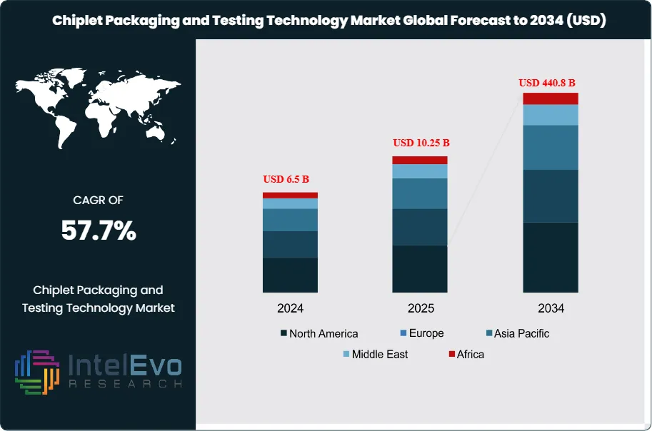
The Chiplet Packaging and Testing Technology Market is estimated at USD 6.5 billion in 2024 and is on track to reach approximately USD 440.8 billion by 2034, implying a robust compound annual growth rate (CAGR) of 57.7% over 2025–2034. This exceptional expansion is being driven by the rapid shift toward modular semiconductor architectures across AI, high-performance computing, and data center platforms, where chiplets enable superior scalability and yield optimization. Rising adoption of advanced 2.5D/3D packaging, heterogeneous integration, and high-bandwidth interconnects is further accelerating market momentum. As leading foundries and OSATs scale capacity to support AI accelerators, automotive electronics, and next-generation computing systems, chiplet packaging and testing is emerging as one of the fastest-growing value pools in the global semiconductor ecosystem.
Get More Information about this report -
Request Free Sample ReportThis extraordinary expansion reflects the growing demand for advanced semiconductor solutions that balance performance, cost, and energy efficiency. The market has shifted rapidly from niche adoption to mainstream relevance, driven by the rising complexity of integrated circuits and the need for modular approaches to chip design. By breaking down monolithic chips into smaller chiplets, manufacturers can reduce costs, improve yields, and accelerate time-to-market while still meeting the performance requirements of high-end computing systems.
Demand-side growth is fueled by industries such as consumer electronics, automotive, telecommunications, and data centers. Each requires high-performance computing capabilities that are both cost-efficient and power-conscious. The surge in artificial intelligence, machine learning, and big data analytics has further intensified the need for specialized processors that chiplet technology can deliver. On the supply side, manufacturers face challenges in ensuring reliable interconnects, maintaining testing accuracy, and managing the capital intensity of advanced packaging facilities. Regulatory scrutiny around semiconductor supply chains and geopolitical risks also add layers of complexity for global players.
Technological progress is reshaping adoption. Advances in interconnect technologies are improving communication between chiplets, while enhanced testing protocols are ensuring reliability at scale. These improvements not only strengthen performance but also reduce manufacturing costs, making chiplet-based architectures more attractive for mass deployment. The technology is also well aligned with the ongoing miniaturization of devices and the requirements of emerging applications such as 5G, IoT, and autonomous vehicles, all of which demand high data throughput and low power consumption.
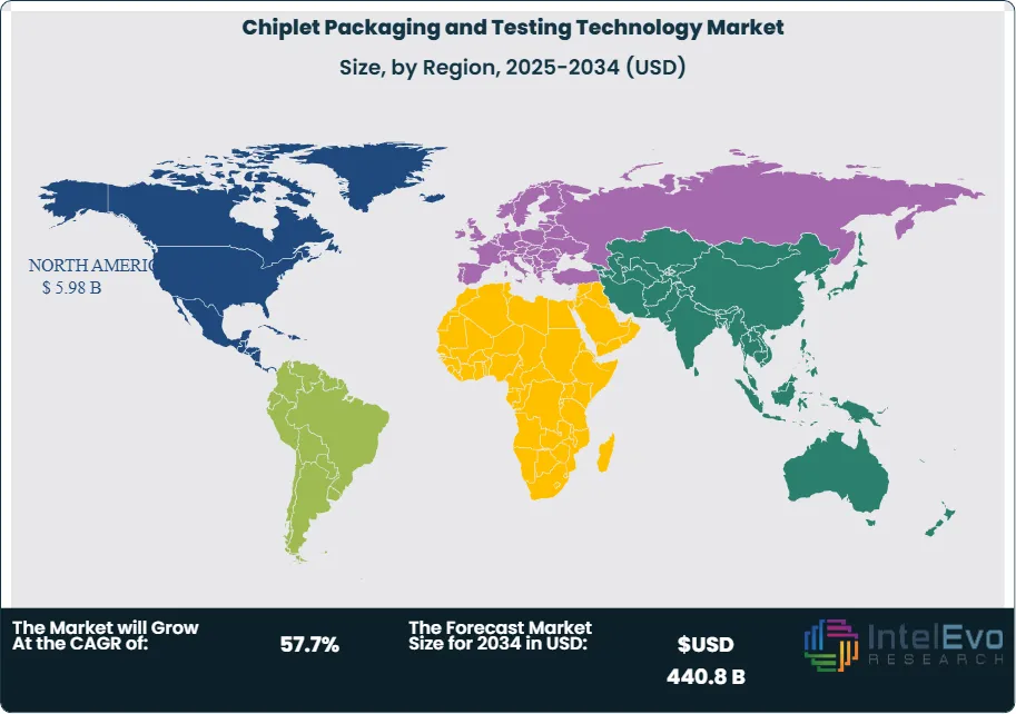
Regionally, Asia-Pacific dominates the market, accounting for 48.6% of global revenue in 2024, or USD 2.6 billion. China alone generated USD 1.38 billion, growing at an annual rate of 56%. This leadership is underpinned by strong domestic demand, government-backed semiconductor initiatives, and the presence of large-scale manufacturing hubs. North America and Europe remain important markets, particularly for high-performance computing and defense applications, while emerging economies in Southeast Asia are expected to attract rising investment as supply chains diversify. For investors, APAC remains the core growth engine, but opportunities are expanding globally as chiplet adoption accelerates across industries.
, By Application (HPC, AI, Automotive, Consumer Electronics), Advanced Interconnect Trends, Supply Chain Dynamics, Key Players & Forecast 2025–2034")
Key Takeaways
- Market Growth: The Chiplet Packaging and Testing Technology Market was valued at USD 6.5 billion in 2024 and is projected to reach USD 440.8 billion by 2034, expanding at a CAGR of 57.7%. Growth is driven by rising demand for high-performance, energy-efficient semiconductors across consumer electronics, automotive, and data center applications.
- Packaging Technology: 3D Packaging led the market in 2024 with a 43.6% share. Its adoption reflects the need for compact, high-density solutions that support advanced computing, automotive electronics, and healthcare devices.
- Testing Method: Pre-Packaging Testing accounted for 55.7% of the market in 2024. This dominance is linked to the critical role of early defect detection in reducing downstream costs and ensuring reliability in high-volume semiconductor production.
- Driver: Consumer electronics represented 34.9% of global demand in 2024. The proliferation of smartphones, wearables, and IoT devices is accelerating adoption of chiplet-based architectures that deliver performance gains while reducing power consumption.
- Restraint: High capital requirements for advanced packaging and testing facilities remain a barrier. Initial setup costs can exceed USD 500 million per facility, limiting entry for smaller players and concentrating market power among established semiconductor manufacturers.
- Opportunity: The automotive sector presents a high-growth opportunity, with chiplet adoption expected to accelerate as electric vehicles and autonomous driving systems demand advanced processors. This segment is projected to grow at a CAGR above 50% through 2034.
- Trend: Advances in interconnect technologies and heterogeneous integration are reshaping the market. Companies such as AMD and Intel are scaling chiplet-based processors for AI and high-performance computing, signaling broader industry adoption.
- Regional Analysis: Asia-Pacific dominated in 2024 with 48.6% of global revenue, or USD 2.6 billion, led by China at USD 1.38 billion with 56% annual growth. North America and Europe remain key for R&D and high-performance applications, while Southeast Asia is emerging as an investment hotspot for manufacturing expansion.
Packaging Type Analysis
In 2025, 3D Packaging continues to dominate the chiplet packaging and testing technology market, accounting for more than 44% of global revenue. Its leadership is reinforced by the growing demand for compact, high-performance semiconductor solutions across data centers, consumer electronics, and automotive applications. By vertically stacking chiplets, 3D Packaging achieves superior interconnect density and reduced silicon footprint, enabling higher bandwidth and lower latency compared to traditional approaches.
The segment’s growth is closely tied to the rising need for computational efficiency in artificial intelligence, cloud infrastructure, and advanced driver-assistance systems. These applications require faster data transfer and lower power consumption, both of which are supported by 3D Packaging architectures. The ability to integrate multiple functions within a single package also enhances system reliability and reduces design complexity, making it a preferred choice for manufacturers seeking performance gains without escalating costs.
Looking ahead, 3D Packaging is expected to maintain its leadership as industries push for miniaturization and higher integration. System-in-Package (SiP) and Fan-Out Wafer-Level Packaging (FOWLP) are also gaining traction, particularly in mobile and IoT devices, but 3D Packaging remains the cornerstone technology for high-performance computing and advanced electronics.
Testing Type Analysis
Pre-Packaging Testing held a commanding 56% share of the market in 2025, underscoring its critical role in ensuring chiplet reliability before final assembly. As chiplet-based designs become more complex, incorporating multiple integrated circuits and advanced materials, early-stage testing has become indispensable for maintaining production yields and reducing downstream costs.
The importance of this segment is amplified by the growing adoption of chiplets in AI accelerators, automotive electronics, and telecommunications infrastructure. In these applications, the failure of a single chiplet can compromise entire systems, making rigorous pre-packaging validation essential. By identifying defects before integration, manufacturers safeguard both performance and profitability, avoiding costly rework at later stages.
Economic efficiency is another driver. Pre-Packaging Testing reduces financial risk by ensuring only functional chiplets move forward to expensive packaging processes. As competition intensifies and time-to-market pressures increase, this testing stage will remain a cornerstone of semiconductor manufacturing strategies.
End-User Industry Analysis
Consumer Electronics continues to lead end-use demand in 2025, representing nearly 35% of global revenue. The segment’s dominance is fueled by the integration of chiplets into smartphones, wearables, gaming consoles, and AR/VR devices, all of which require compact yet powerful processing capabilities. The modular nature of chiplets allows manufacturers to deliver higher performance in smaller device footprints, aligning with the ongoing miniaturization trend in electronics.
The rise of immersive technologies such as AR and VR, alongside high-performance gaming, has further accelerated adoption. These applications demand advanced GPU and CPU configurations, which chiplets enable through flexible and efficient architectures. Additionally, the proliferation of IoT and smart devices has expanded the role of chiplets in enabling faster connectivity and seamless device integration.
While consumer electronics leads, automotive and healthcare are emerging as high-growth segments. Electric vehicles and autonomous driving systems require advanced processors for real-time data processing, while medical imaging and diagnostic devices increasingly rely on chiplet-based solutions for precision and efficiency.
Regional Analysis
Asia Pacific remains the largest regional market in 2025, accounting for nearly half of global revenue. China continues to lead within the region, supported by government-backed semiconductor initiatives, strong domestic demand, and large-scale manufacturing capacity. In 2025, China’s chiplet packaging and testing market is estimated to exceed USD 1.6 billion, growing at an annual rate above 50%.
North America follows as a key hub for R&D and high-performance computing applications. Companies such as AMD, Intel, and NVIDIA are driving adoption through chiplet-based processors designed for AI, cloud, and data center workloads. Europe also plays a significant role, particularly in automotive and industrial applications, where demand for reliable and energy-efficient semiconductors is accelerating.
Emerging markets in Southeast Asia and the Middle East are attracting rising investment as global supply chains diversify. Countries such as Vietnam, Malaysia, and the UAE are positioning themselves as alternative manufacturing and testing hubs, offering cost advantages and strategic proximity to major electronics markets. This regional diversification is expected to shape the competitive landscape through 2030 and beyond.
Get More Information about this report -
Request Free Sample ReportMarket Key Segments
By Packaging Type
- 2.5D Packaging
- 3D Packaging
- System-in-Package (SiP)
- Fan-Out Wafer-Level Packaging (FOWLP)
By Testing Type
- Pre-Packaging Testing
- Post-Packaging Testing
By End-User Industry
- Consumer Electronics
- Automotive
- Telecommunications
- Industrial
- Healthcare
- Others
Regions
- North America
- Latin America
- East Asia And Pacific
- Sea And South Asia
- Eastern Europe
- Western Europe
- Middle East & Africa
| Report Attribute | Details |
| Market size (2024) | USD 6.5 B |
| Forecast Revenue (2034) | USD 440.8 B |
| CAGR (2024-2034) | 57.7% |
| Historical data | 2020-2023 |
| Base Year For Estimation | 2024 |
| Forecast Period | 2025-2034 |
| Report coverage | Revenue Forecast, Competitive Landscape, Market Dynamics, Growth Factors, Trends and Recent Developments |
| Segments covered | By Packaging Type (2.5D Packaging, 3D Packaging, System-in-Package (SiP), Fan-Out Wafer-Level Packaging (FOWLP)), By Testing Type (Pre-Packaging Testing, Post-Packaging Testing), By End-User Industry (Consumer Electronics, Automotive, Telecommunications, Industrial, Healthcare, Others) |
| Research Methodology |
|
| Regional scope |
|
| Competitive Landscape | Samsung Electronics, Advanced Micro Devices Inc. (AMD), Amkor Technology Inc., Broadcom Inc., Intel Corporation, Qualcomm Incorporated, NVIDIA Corporation, TSMC (Taiwan Semiconductor Manufacturing Company), Advanced Semiconductor Engineering Inc. (ASE Group) |
| Customization Scope | Customization for segments, region/country-level will be provided. Moreover, additional customization can be done based on the requirements. |
| Pricing and Purchase Options | Avail customized purchase options to meet your exact research needs. We have three licenses to opt for: Single User License, Multi-User License (Up to 5 Users), Corporate Use License (Unlimited User and Printable PDF). |
, By Application (HPC, AI, Automotive, Consumer Electronics), Advanced Interconnect Trends, Supply Chain Dynamics, Key Players & Forecast 2025–2034")
, By Application (HPC, AI, Automotive, Consumer Electronics), Advanced Interconnect Trends, Supply Chain Dynamics, Key Players & Forecast 2025–2034")
, By Application (HPC, AI, Automotive, Consumer Electronics), Advanced Interconnect Trends, Supply Chain Dynamics, Key Players & Forecast 2025–2034")
Frequently Asked Questions
How big is the Chiplet Packaging and Testing Technology Market?
The Chiplet Packaging and Testing Technology Market was valued at USD 6.5 billion in 2024 and is projected to reach USD 440.8 billion by 2034, growing at a remarkable 57.7% CAGR during 2024–2034. Rapid adoption of chiplet-based architectures in AI, high-performance computing, data centers, and advanced automotive electronics is driving demand for 2.5D/3D packaging, heterogeneous integration, and high-bandwidth interconnect technologies.
Who are the major players in the Chiplet Packaging and Testing Technology Market?
Samsung Electronics, Advanced Micro Devices Inc. (AMD), Amkor Technology Inc., Broadcom Inc., Intel Corporation, Qualcomm Incorporated, NVIDIA Corporation, TSMC (Taiwan Semiconductor Manufacturing Company), Advanced Semiconductor Engineering Inc. (ASE Group)
Which segments covered the Chiplet Packaging and Testing Technology Market?
By Packaging Type (2.5D Packaging, 3D Packaging, System-in-Package (SiP), Fan-Out Wafer-Level Packaging (FOWLP)), By Testing Type (Pre-Packaging Testing, Post-Packaging Testing), By End-User Industry (Consumer Electronics, Automotive, Telecommunications, Industrial, Healthcare, Others)
How can this market research report help my business make strategic decisions?
Our market research reports provide actionable intelligence, including verified market size data, CAGR projections, competitive benchmarking, and segment-level opportunity analysis. These insights support strategic planning, investment decisions, product development, and market entry strategies for enterprises and startups alike.
How frequently is the data updated?
We continuously monitor industry developments and update our reports to reflect regulatory changes, technological advancements, and macroeconomic shifts. Updated editions ensure you receive the latest market intelligence.

Select Licence Type
Connect with our sales team
Chiplet Packaging and Testing Technology Market
Published Date : 31 Dec 2025 | Formats :Why IntelEvoResearch
100%
Customer
Satisfaction
24x7+
Availability - we are always
there when you need us
200+
Fortune 50 Companies trust
IntelEvoResearch
80%
of our reports are exclusive
and first in the industry
100%
more data
and analysis
1000+
reports published
till date
