
- Home
- Industries
 Aerospace And Defence
 Agriculture
 Automotive And Transportation
 Banking And Finance
 Business
 Chemicals And Materials
 Consumer And Retail
 Electronics And Semiconductors
 Food And Beverages
 Machinery & Equipments
 Manufacturing And Construction
 Medical Devices
 Others
 Pharmaceuticals And Healthcare
 Power And Energy
 Sports
 Technology
- Services
- News Room
- About us
- Contact Us
-
Electron Beam Lithography System Market Size | 8.8% CAGR
Global Electron Beam Lithography System Market Size, Share & Analysis Type (Gaussian beam EBL Systems, Shaped beam EBL Systems), By Application (Academic Field, Industrial Field), By End User (Research institutions, Academic laboratories) Industry Outlook, Chip Miniaturization Trends & Forecast 2025–2034

Report Overview
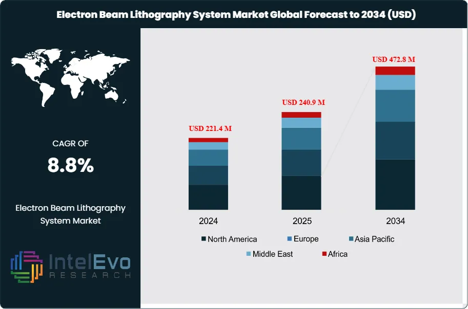
The Electron Beam Lithography (EBL) System Market is estimated at USD 221.4 million in 2024 and is projected to reach approximately USD 472.8 million by 2034, registering a CAGR of about 8.8% during 2025–2034. This growth is supported by rising demand for ultra-high-resolution patterning in advanced semiconductor R&D, photonics, quantum devices, and nanotechnology applications. Increasing investments in sub-5 nm node research, compound semiconductors, and academic–industrial nanofabrication centers are reinforcing long-term adoption. Additionally, EBL’s critical role in prototyping next-generation chips and nano-devices positions the market as a strategic enabler within the evolving advanced manufacturing ecosystem.
Get More Information about this report -
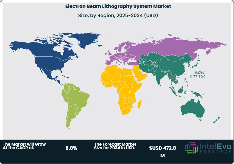
Request Free Sample ReportIn 2023, the Asia-Pacific region led the market, accounting for 35.1% of the total share with a revenue of USD 68.8 million, driven by significant investments in semiconductor manufacturing and nanotechnology infrastructure.
Electron Beam Lithography systems are critical tools in nanofabrication, enabling the creation of intricate patterns with sub-10-nanometer resolution. Their precision and versatility have positioned them as essential components in industries such as semiconductor manufacturing, photonics, and advanced research. The market's growth is fueled by increasing demand for miniaturized electronic devices, which require sophisticated manufacturing technologies capable of producing complex nanoscale components. Furthermore, the expanding applications of nanotechnology in medicine, energy, and materials science are driving the adoption of EBL systems across various sectors.
The rapid evolution of the semiconductor industry and the rising complexity of electronic devices significantly contribute to market expansion. As devices become smaller and more advanced, the stringent requirements for high-resolution patterning and reliable nanofabrication techniques intensify the demand for EBL systems. Additionally, the growing focus on quantum computing, which relies on precise fabrication of quantum devices, is creating new avenues for market growth.
Technological advancements continue to shape the EBL market, making these systems more efficient and accessible. Innovations in electron beam control, resist materials, and software interfaces are driving improvements in throughput and cost-effectiveness, without compromising precision. These advancements are expected to broaden the scope of EBL applications, particularly in emerging fields like biosensors and nanoscale biological tools.
Regionally, Asia-Pacific remains a key investment hotspot, driven by robust infrastructure development and government initiatives supporting nanotechnology research. Meanwhile, North America and Europe are also witnessing steady growth, supported by advancements in quantum computing and R&D activities. Emerging markets in Latin America and the Middle East present additional opportunities, as investments in technological infrastructure and nanotechnology gain momentum. With increasing demand across diverse applications, the electron beam lithography system market is expected to maintain a strong growth trajectory through 2034.
, By Application (Academic Field, Industrial Field), By End User (Research institutions, Academic laboratories) Industry Outlook, Chip Miniaturization Trends & Forecast 2025–2034")
Key Takeaways
- Market Growth: The Electron Beam Lithography (EBL) System market is projected to grow at a CAGR of 8.8% from 2025 to 2034, increasing from USD 221.4 million in 2024 to USD 472.8 million by 2034. This growth is driven by rising demand for high-resolution nanofabrication tools in electronics, photonics, and quantum computing.
- Product Type (Shaped Beam EBL Systems): Shaped Beam EBL Systems led the market in 2023, accounting for over 67.4% of total revenue. Their dominance is attributed to superior precision, resolution, and patterning fidelity, making them the preferred choice for advanced applications.
- End Use (Industrial Applications): The Industrial Field segment held a commanding 78.9% market share in 2023, supported by increasing demand for advanced electronic components and sustained R&D investments in semiconductors and nanotechnology.
- Driver: The miniaturization of electronic devices is a key growth driver. As devices require increasingly smaller components, the demand for highly sophisticated nanofabrication tools like EBL systems has surged. This trend is further amplified by the rapid growth of quantum computing and photonics industries.
- Restraint: High system costs and low throughput remain significant barriers to adoption. Many smaller organizations struggle with the affordability of EBL systems, limiting their accessibility outside of well-funded industrial and academic sectors.
- Opportunity: Emerging applications in biosensors and nanoscale biological tools present untapped potential for market growth. These nontraditional uses are expected to gain traction, particularly in the medical and life sciences sectors, as advancements in nanotechnology continue.
- Trend: Advances in beam control, resist materials, and automation are improving the efficiency and usability of EBL systems. Companies such as NanoBeam Ltd. and Raith GmbH are focusing on developing cost-effective solutions to expand adoption across broader markets.
- Regional Analysis: Asia-Pacific dominated the market in 2023, capturing more than 35.1% of total revenue. This leadership is driven by robust electronics manufacturing, nanotechnology advancements, and favorable government initiatives in China, Japan, and South Korea. North America and Europe are also poised for significant growth due to increasing investments in quantum computing and semiconductor R&D.
Type Analysis
In 2025, Shaped Beam Electron Beam Lithography (EBL) Systems remain the leading segment in the global EBL market, accounting for over 67% of the total market share.
This dominance stems from their superior capabilities compared to Gaussian Beam EBL Systems, particularly in precision and scalability. Shaped Beam systems utilize a customizable electron beam that allows for intricate and highly controlled pattern formation, making them indispensable for advanced nanofabrication processes.
One of the primary advantages of Shaped Beam EBL Systems is their ability to achieve sub-10-nanometer resolution, a critical requirement for semiconductor manufacturing, photonics, and other industries demanding intricate nanoscale patterns. Furthermore, these systems excel in mitigating the proximity effect, a phenomenon where scattered electrons cause distortions in adjacent features. Shaped Beam EBL Systems deploy advanced correction techniques to ensure pattern fidelity, enhancing their appeal in high-precision applications.
Additionally, Shaped Beam EBL Systems are extensively used in research and development settings, including academic institutions, government laboratories, and cutting-edge technology firms. Their versatility makes them a preferred choice for exploring next-generation materials and devices, cementing their role as a driving force in technological advancements. As demand for miniaturized components and high-resolution technologies grows, the Shaped Beam segment is poised to maintain its market leadership.
Application Analysis
The Industrial Field segment continues to dominate the EBL market in 2025, capturing more than 78% of the global market share. This segment benefits significantly from the growing demand for advanced lithography systems in industries such as semiconductors, nanotechnology, and optoelectronics. As manufacturers push the boundaries of nanoscale production, EBL systems have become indispensable for creating precise and complex patterns required in these high-tech fields.
The increasing adoption of technologies such as Internet of Things (IoT), artificial intelligence (AI), and 5G connectivity has intensified the need for smaller, more efficient electronic components. Electron beam lithography systems enable manufacturers to produce miniaturized transistors, sensors, and photonic devices, which are essential for these emerging technologies. This trend has been further bolstered by investments in R&D, as companies collaborate with academic institutions to drive innovation in lithography techniques and improve system performance.
Moreover, the Industrial Field segment benefits from economies of scale, as high-volume production and bulk purchases lower overall costs. This has made EBL systems more accessible to industrial players, solidifying their dominance in the market. With the continued growth of advanced manufacturing sectors, the Industrial Field segment is expected to sustain its leading position through 2030.
End-Use Analysis
In 2025, the semiconductor industry remains the largest end-use sector for EBL systems, driven by the demand for high-performance chips in applications ranging from consumer electronics to autonomous vehicles. The continuous push for node shrinkage in semiconductor manufacturing has necessitated the adoption of EBL systems capable of delivering nanometer-level accuracy.
Research institutions and academic laboratories also represent a significant segment in the EBL market. These entities leverage the precision of EBL systems to develop innovative materials and devices, including quantum computing components and nanophotonic structures. The flexibility of EBL systems in supporting exploratory science and technology development ensures their widespread use in these settings.
Additionally, the medical device industry is emerging as a key end-use market. EBL systems are increasingly applied in the production of microfluidic devices, biosensors, and drug delivery systems, which require precise micro- and nano-scale architectures. With healthcare innovation accelerating globally, this segment is poised for substantial growth in the coming years.
Regional Analysis
The Asia-Pacific region continues to lead the global EBL market in 2025, commanding over 35% market share. The region’s dominance can be attributed to its robust electronics manufacturing sector, with countries like China, South Korea, and Taiwan at the forefront of semiconductor production. In 2025, the demand for EBL systems in Asia-Pacific is projected to exceed USD 80 million, driven by the growing need for high-resolution lithography in consumer electronics and telecommunications.
Asia-Pacific’s leadership is further reinforced by significant investments in nanotechnology and R&D activities. Governments in the region, particularly in China and Japan, have introduced strategic initiatives to boost the adoption of advanced manufacturing technologies, including EBL systems. For instance, China’s “Made in China 2025” policy and South Korea’s technology innovation programs have created a supportive environment for market growth.
Additionally, the region is experiencing rapid growth in emerging technologies such as augmented reality (AR), virtual reality (VR), and 5G infrastructure, all of which rely on miniaturized components manufactured using EBL systems. With continued advancements in these areas, the Asia-Pacific market is expected to maintain its leading position, while regions like North America and Europe will witness gradual growth fueled by investments in cutting-edge research and semiconductor manufacturing.
Get More Information about this report -
Request Free Sample ReportMarket Key Segments
Type
- Gaussian beam EBL Systems
- Shaped beam EBL Systems
Application
- Academic Field
- Industrial Field
End User
- Research institutions
- Academic laboratories
Regions
- North America
- Latin America
- East Asia And Pacific
- Sea And South Asia
- Eastern Europe
- Western Europe
- Middle East & Africa
| Report Attribute | Details |
| Market size (2024) | USD 221.4 M |
| Forecast Revenue (2034) | USD 472.8 M |
| CAGR (2024-2034) | 8.8% |
| Historical data | 2020-2023 |
| Base Year For Estimation | 2024 |
| Forecast Period | 2025-2034 |
| Report coverage | Revenue Forecast, Competitive Landscape, Market Dynamics, Growth Factors, Trends and Recent Developments |
| Segments covered | Type (Gaussian beam EBL Systems, Shaped beam EBL Systems), By Application (Academic Field, Industrial Field), By End User (Research institutions, Academic laboratories) |
| Research Methodology |
|
| Regional scope |
|
| Competitive Landscape | JEOL, Ltd., Raith GmbH, IMS Nanofabrication GmbH, STS-Elionix, NanoBeam Ltd., Nanoscribe GmbH, Vistec Electron Beam GmbH, CRESTEC Corporation, NIL Technology ApS, JC Nabity Lithography Systems, Other Key Players |
| Customization Scope | Customization for segments, region/country-level will be provided. Moreover, additional customization can be done based on the requirements. |
| Pricing and Purchase Options | Avail customized purchase options to meet your exact research needs. We have three licenses to opt for: Single User License, Multi-User License (Up to 5 Users), Corporate Use License (Unlimited User and Printable PDF). |
, By Application (Academic Field, Industrial Field), By End User (Research institutions, Academic laboratories) Industry Outlook, Chip Miniaturization Trends & Forecast 2025–2034")
, By Application (Academic Field, Industrial Field), By End User (Research institutions, Academic laboratories) Industry Outlook, Chip Miniaturization Trends & Forecast 2025–2034")
, By Application (Academic Field, Industrial Field), By End User (Research institutions, Academic laboratories) Industry Outlook, Chip Miniaturization Trends & Forecast 2025–2034")

Select Licence Type
Connect with our sales team
Electron Beam Lithography System Market
Published Date : 23 Dec 2025 | Formats :Why IntelEvoResearch
100%
Customer
Satisfaction
24x7+
Availability - we are always
there when you need us
200+
Fortune 50 Companies trust
IntelEvoResearch
80%
of our reports are exclusive
and first in the industry
100%
more data
and analysis
1000+
reports published
till date
