
- Home
- Industries
 Aerospace And Defence
 Agriculture
 Automotive And Transportation
 Banking And Finance
 Business
 Chemicals And Materials
 Consumer And Retail
 Electronics And Semiconductors
 Food And Beverages
 Machinery & Equipments
 Manufacturing And Construction
 Medical Devices
 Others
 Pharmaceuticals And Healthcare
 Power And Energy
 Sports
 Technology
- Services
- News Room
- About us
- Contact Us
-
Electron Microscope Market Size, Growth Trends & Forecast | CAGR 6.8%
Global Electron Microscope Market Size, Share & Imaging Technology Analysis By Type (SEM, TEM, STEM), By Application (Life Sciences, Semiconductors, Materials Science), By End User (Research Labs, Academia, Industry), AI-Enabled Microscopy Trends, Regional Outlook & Forecast 2025–2034

Report Overview
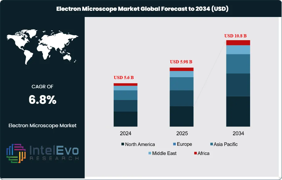
The Electron Microscope Market is estimated at USD 5.6 billion in 2024 and is projected to reach approximately USD 10.8 billion by 2034, registering a compound annual growth rate (CAGR) of about 6.8% during 2025–2034. This steady expansion is driven by rising demand for high-resolution imaging across semiconductor manufacturing, materials science, nanotechnology, and life sciences research. Increasing investments in advanced R&D infrastructure, growth in chip fabrication and failure analysis, and wider adoption of electron microscopy in drug discovery and structural biology are reinforcing long-term market momentum.
Get More Information about this report -
Request Free Sample ReportThis growth reflects a steady expansion in demand across both academic and industrial applications. Historically, electron microscopes were confined to specialized research laboratories, but over the past decade adoption has broadened as industries such as semiconductors, materials science, and life sciences have integrated advanced imaging into core workflows. The COVID-19 pandemic accelerated this trend, with electron microscopes playing a critical role in virus characterization, vaccine development, and drug discovery.
The market’s trajectory is shaped by both demand-side and supply-side factors. On the demand side, rising investment in nanotechnology, semiconductor miniaturization, and structural biology continues to expand the user base. The semiconductor sector alone accounted for more than 30% of global demand in 2022, driven by the need for atomic-level inspection of integrated circuits. On the supply side, manufacturers face challenges related to high capital costs, complex maintenance requirements, and the shortage of skilled operators. These barriers limit penetration in smaller laboratories and emerging economies, although rental models and shared research facilities are helping to bridge the gap.
Technology is reshaping adoption patterns. Advances in digital imaging, automation, and artificial intelligence are reducing analysis time and improving accuracy. Automated sample handling and AI-driven image recognition are enabling faster throughput in pharmaceutical research and semiconductor quality control. Integration with cloud-based platforms is also gaining traction, allowing remote collaboration and data sharing across research teams. These developments are making electron microscopy more accessible and efficient for end users.
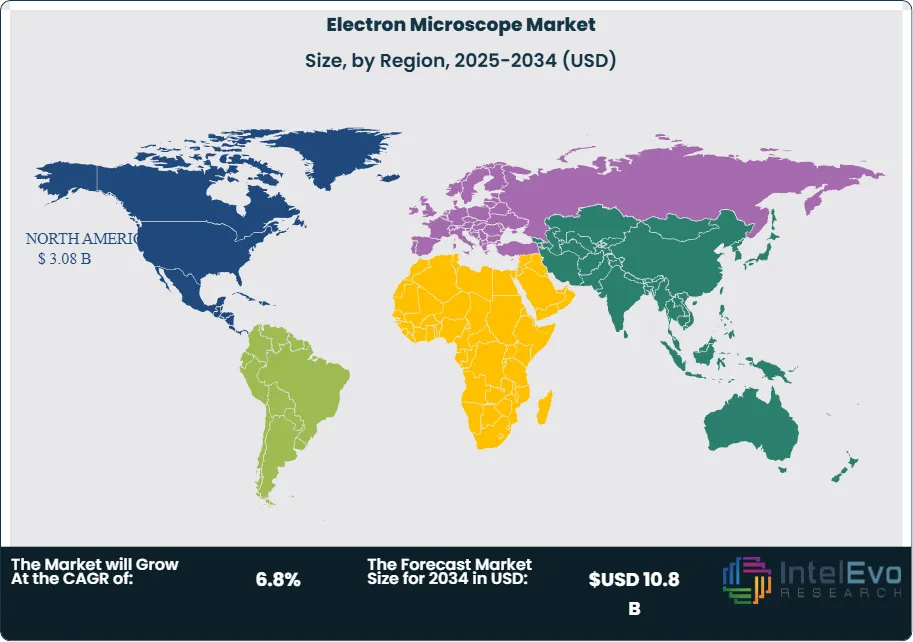
Regionally, North America and Europe remain the largest markets, supported by strong research funding and established semiconductor and biotechnology industries. The United States alone accounts for nearly 35% of global revenue, reflecting its concentration of pharmaceutical and nanotechnology research. Asia-Pacific, however, is the fastest-growing region, with China, Japan, and South Korea investing heavily in semiconductor fabrication and advanced materials research. India is also emerging as a key growth market, supported by government-backed R&D initiatives. For investors, Asia-Pacific represents the most attractive opportunity over the forecast period, while established markets in North America and Europe will continue to provide steady returns through incremental upgrades and replacement demand.
, By Application (Life Sciences, Semiconductors, Materials Science), By End User (Research Labs, Academia, Industry), AI-Enabled Microscopy Trends, Regional Outlook & Forecast 2025–2034")
Key Takeaways
- Market Growth: The global electron microscope market was valued at USD 5.6 billion in 2024 and is projected to reach USD 10.8 billion by 2034, expanding at a CAGR of 9.14%. Growth is driven by rising demand in semiconductors, nanotechnology, and life sciences research.
- Product Type: Scanning Electron Microscopes (SEM) accounted for over 40% of total revenue in 2023, supported by widespread use in materials science and biological imaging. Their cost-effectiveness and versatility make them the preferred choice across academic and industrial laboratories.
- Application: Semiconductor and electronics applications represented more than 30% of global demand in 2022, fueled by the need for atomic-level inspection of integrated circuits. The sector continues to expand as chipmakers invest in advanced fabrication technologies.
- Driver: Rising investment in structural biology and drug discovery is accelerating adoption. Cryo-electron microscopy (Cryo-EM) has become a critical tool in pharmaceutical R&D, with global Cryo-EM installations increasing by more than 15% annually since 2020.
- Restraint: High acquisition costs, often exceeding USD 1 million per unit, and ongoing maintenance expenses restrict adoption among smaller institutions. The shortage of skilled operators further limits accessibility, particularly in emerging economies.
- Opportunity: Asia-Pacific presents the strongest growth potential, with the market expected to expand at a CAGR above 10% through 2032. Government-backed R&D programs in China, Japan, and India are creating demand for advanced microscopy solutions.
- Trend: Integration of artificial intelligence and machine learning into electron microscopy is improving image analysis speed and accuracy. Companies such as Thermo Fisher Scientific and Carl Zeiss are embedding AI-driven software into new product lines to enhance throughput.
- Regional Analysis: North America and Europe together accounted for more than 55% of global revenue in 2023, supported by strong research funding and established semiconductor industries. Asia-Pacific is the fastest-growing region, projected to surpass 30% of global share by 2032, making it the key investment hotspot for the next decade.
Type Analysis
The electron microscope market in 2025 remains primarily divided between Scanning Electron Microscopes (SEM) and Transmission Electron Microscopes (TEM). SEM continues to hold the largest share, accounting for more than 45% of global revenue, supported by its versatility across materials science, nanotechnology, and life sciences. The segment is projected to expand at a CAGR of around 8.3% through 2032, driven by demand for high-resolution surface imaging in semiconductor fabrication and advanced materials research.
SEM technology enables three-dimensional visualization of surfaces at nanoscale precision, making it indispensable for analyzing metals, polymers, ceramics, and biological samples. Its ability to provide detailed morphology and topography has positioned it as the preferred choice for both industrial quality control and academic research. In contrast, TEM adoption is accelerating in structural biology and pharmaceutical research, where atomic-level imaging is critical. TEM’s ability to resolve internal structures of cells, tissues, and nanomaterials is fueling demand, particularly in drug discovery and protein analysis.
Looking ahead, both SEM and TEM will benefit from integration with digital imaging and AI-driven analytics. SEM will remain dominant in industrial applications, while TEM is expected to capture greater share in healthcare and nanotechnology, supported by rising R&D investments and government-backed research programs.
Application Analysis
Materials science continues to represent the largest application segment, accounting for nearly 35% of total market demand in 2024. Researchers rely on electron microscopes to characterize metals, ceramics, composites, and polymers at the nanoscale, supporting industries such as aerospace, automotive, and energy storage. The need for advanced materials with higher strength-to-weight ratios and improved conductivity is sustaining long-term demand.
Life sciences represent the fastest-growing application, with a projected CAGR above 9% through 2032. Cryo-electron microscopy has become a cornerstone in structural biology, enabling visualization of proteins, DNA, and RNA at near-atomic resolution. This capability is accelerating drug discovery pipelines and vaccine development, with pharmaceutical companies and research institutes expanding their adoption of high-end TEM systems.
Nanotechnology is also emerging as a critical growth area. Electron microscopes are essential for visualizing nanoparticles, nanotubes, and quantum materials, which are increasingly used in electronics, energy storage, and medical devices. As global nanomaterials production scales, demand for advanced microscopy solutions will continue to rise.
End-Use Analysis
The commercial sector, particularly semiconductor and electronics manufacturing, accounts for the largest share of end-use demand. In 2024, semiconductor applications represented more than 30% of total revenue, reflecting the industry’s reliance on nanoscale inspection for integrated circuit design and fabrication. Continued investment in advanced chipmaking facilities in Asia and North America will sustain this trend.
The residential and academic research segment is expanding steadily, supported by government-funded laboratories and university research centers. Shared microscopy facilities are making high-cost instruments more accessible, particularly in Europe and Asia-Pacific. This model is helping smaller institutions participate in advanced research without the burden of direct capital expenditure.
Industrial applications, including metallurgy, mining, and energy, are also contributing to growth. Electron microscopes are increasingly used to analyze material degradation, corrosion, and structural performance, supporting industries focused on sustainability and long-term durability.
Regional Analysis
North America and Europe remain the largest markets, together accounting for more than 55% of global revenue in 2024. The United States leads with strong demand from pharmaceutical research, nanotechnology, and semiconductor industries, while Europe benefits from established academic and government-funded research programs.
Asia-Pacific is the fastest-growing region, projected to expand at a CAGR above 10% through 2032. China, Japan, and South Korea are investing heavily in semiconductor fabrication and advanced materials research, driving large-scale adoption of both SEM and TEM systems. India is also emerging as a key growth hub, supported by government-backed R&D initiatives and expanding biotech research.
Latin America and the Middle East & Africa remain smaller markets but are showing steady adoption, particularly in mining, materials testing, and academic research. As infrastructure and research funding expand, these regions are expected to provide incremental growth opportunities for global manufacturers.
Get More Information about this report -
Request Free Sample ReportMarket Key Segments
By Type
- Scanning Electron Microscope
- Transmission Electron Microscope
By Application
- Life Science
- Material Science
- Nanotechnology
- Semiconductors
- Others
Regions
- North America
- Latin America
- East Asia And Pacific
- Sea And South Asia
- Eastern Europe
- Western Europe
- Middle East & Africa
| Report Attribute | Details |
| Market size (2024) | USD 5.6 B |
| Forecast Revenue (2034) | USD 10.8 B |
| CAGR (2024-2034) | 6.8% |
| Historical data | 2020-2023 |
| Base Year For Estimation | 2024 |
| Forecast Period | 2025-2034 |
| Report coverage | Revenue Forecast, Competitive Landscape, Market Dynamics, Growth Factors, Trends and Recent Developments |
| Segments covered | By Type (Scanning Electron Microscope, Transmission Electron Microscope), By Application (Life Science, Material Science, Nanotechnology, Semiconductors, Others) |
| Research Methodology |
|
| Regional scope |
|
| Competitive Landscape | Carl Zeiss AG, Nikon Instruments Inc., Thermo Fisher Scientific Inc., Olympus Corp., Bruker Corporation, Leica Microsystems, Hitachi High-Technologies Corporation, JEOL Ltd. |
| Customization Scope | Customization for segments, region/country-level will be provided. Moreover, additional customization can be done based on the requirements. |
| Pricing and Purchase Options | Avail customized purchase options to meet your exact research needs. We have three licenses to opt for: Single User License, Multi-User License (Up to 5 Users), Corporate Use License (Unlimited User and Printable PDF). |
, By Application (Life Sciences, Semiconductors, Materials Science), By End User (Research Labs, Academia, Industry), AI-Enabled Microscopy Trends, Regional Outlook & Forecast 2025–2034")
, By Application (Life Sciences, Semiconductors, Materials Science), By End User (Research Labs, Academia, Industry), AI-Enabled Microscopy Trends, Regional Outlook & Forecast 2025–2034")
, By Application (Life Sciences, Semiconductors, Materials Science), By End User (Research Labs, Academia, Industry), AI-Enabled Microscopy Trends, Regional Outlook & Forecast 2025–2034")
Frequently Asked Questions
How big is the Electron Microscope Market?
The Electron Microscope Market is valued at USD 5.6 billion in 2024 and is projected to reach USD 10.8 billion by 2034, growing at a 6.8% CAGR during 2025–2034. Market growth is driven by rising demand for high-resolution imaging in semiconductor manufacturing, materials science, nanotechnology, and life sciences, alongside increasing R&D investments and expanding applications in drug discovery and failure analysis.
Who are the major players in the Electron Microscope Market?
Carl Zeiss AG, Nikon Instruments Inc., Thermo Fisher Scientific Inc., Olympus Corp., Bruker Corporation, Leica Microsystems, Hitachi High-Technologies Corporation, JEOL Ltd.
Which segments covered the Electron Microscope Market?
By Type (Scanning Electron Microscope, Transmission Electron Microscope), By Application (Life Science, Material Science, Nanotechnology, Semiconductors, Others)
How can this market research report help my business make strategic decisions?
Our market research reports provide actionable intelligence, including verified market size data, CAGR projections, competitive benchmarking, and segment-level opportunity analysis. These insights support strategic planning, investment decisions, product development, and market entry strategies for enterprises and startups alike.
How frequently is the data updated?
We continuously monitor industry developments and update our reports to reflect regulatory changes, technological advancements, and macroeconomic shifts. Updated editions ensure you receive the latest market intelligence.

Select Licence Type
Connect with our sales team
Why IntelEvoResearch
100%
Customer
Satisfaction
24x7+
Availability - we are always
there when you need us
200+
Fortune 50 Companies trust
IntelEvoResearch
80%
of our reports are exclusive
and first in the industry
100%
more data
and analysis
1000+
reports published
till date
