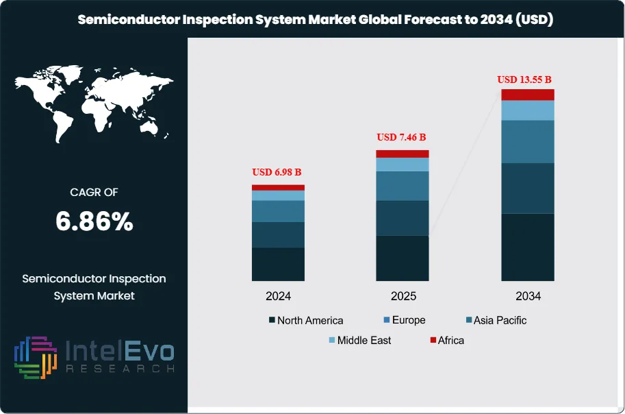
The Semiconductor Inspection System Market size is expected to be worth around USD 13.55 Billion by 2034, from USD 6.98 Billion in 2024, growing at a CAGR of 6.86% during the forecast period from 2024 to 2034. The Semiconductor Inspection System Market encompasses sophisticated equipment and technologies used to examine semiconductor devices, wafers, and components for defects, dimensional accuracy, and quality compliance throughout the manufacturing process. These systems integrate advanced optical, e-beam, and machine vision technologies to ensure the integrity and performance of semiconductor products at various production stages, including wafer fabrication, lithography, etching, and assembly processes.
The market is experiencing robust expansion driven by the exponential demand for miniaturized, high-performance semiconductors across consumer electronics, automotive, telecommunications, and industrial applications. The proliferation of artificial intelligence, Internet of Things (IoT), 5G networks, and advanced driver assistance systems (ADAS) has created unprecedented requirements for precision semiconductor manufacturing. Additionally, the transition to smaller node technologies and three-dimensional integrated circuits necessitates increasingly sophisticated inspection capabilities to maintain yield rates and product reliability.
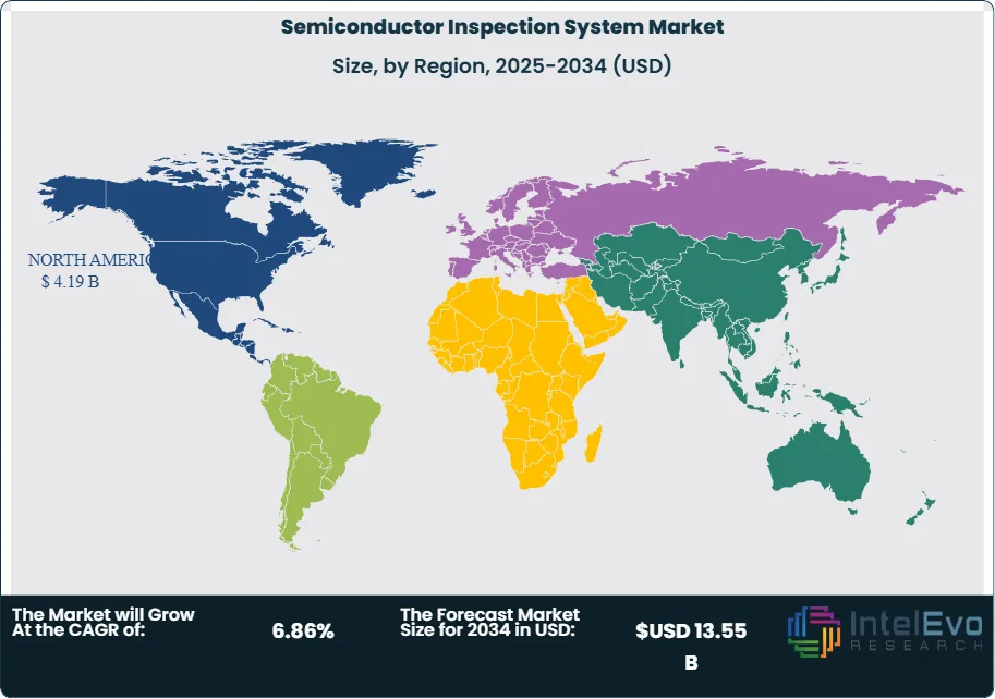
Asia-Pacific dominates the global semiconductor inspection system market, accounting for the largest revenue share due to the concentration of major semiconductor manufacturing facilities in countries like Taiwan, South Korea, China, and Japan. The region benefits from significant investments in semiconductor fabrication capacity, government support for technology advancement, and the presence of leading foundries and integrated device manufacturers. North America maintains a strong position through technological innovation, research and development capabilities, and the presence of major inspection equipment manufacturers.
The pandemic initially disrupted semiconductor supply chains and manufacturing operations, leading to temporary delays in equipment procurement and installation. However, the accelerated digital transformation, increased demand for electronic devices, and the critical importance of semiconductor supply chain resilience have driven sustained investment in inspection equipment. The pandemic highlighted the strategic importance of semiconductor manufacturing capabilities, leading to increased government support and private investment in advanced inspection technologies.
Ongoing trade tensions and technology restrictions have significantly influenced the semiconductor inspection system market, with governments implementing export controls on advanced semiconductor manufacturing equipment. These restrictions have prompted regional diversification of supply chains, increased domestic manufacturing capabilities, and accelerated development of indigenous inspection technologies. The geopolitical landscape has created opportunities for regional players while challenging established global supply chain models.
Key Takeaways
Market Growth: The Semiconductor Inspection System Market is expected to reach USD 13.55 Billion by 2034, due to demand for compact, high-performance semiconductors across various sectors like consumer electronics, automotive, and telecommunications is driving market expansion.
Product Type Dominance: Wafer Inspection Systems lead the market due to critical role in yield optimization and defect detection.
Technology Dominance: Optical Inspection dominates the market, driven by high-speed capabilities and versatility across applications.
End-User Dominance: Foundries hold the largest market share, due to their central role in wafer fabrication and their investments in cutting-edge inspection technologies.
Drivers: Key drivers accelerating growth include semiconductor miniaturization and advanced node adoption, which boost market expansion through increased inspection complexity and precision requirements.
Restraints: Growth is hindered by high equipment costs and technical complexity, which create challenges such as capital constraints and integration difficulties.
Opportunities: The market is poised for expansion due to opportunities like AI-powered inspection systems and emerging semiconductor applications, which enable enhanced defect detection and new market segments.
Trends: Emerging trends including machine learning integration and multi-modal inspection approaches are reshaping the market by improving accuracy and comprehensive defect analysis.
Regional Leader: Asia-Pacific leads owing to semiconductor manufacturing concentration and foundry investments. North America and Europe show high promise due to technology innovation and strategic semiconductor initiatives.
Product Type Analysis:
The Product Type segment represents the core inspection technologies that define system capabilities and application suitability across semiconductor manufacturing processes. Wafer Inspection Systems maintain market dominance due to their fundamental role in detecting defects, monitoring process variations, and ensuring yield optimization throughout semiconductor fabrication. These systems excel in high-volume production environments where consistent quality control is paramount for maintaining profitability and meeting stringent industry standards. Mask Inspection Systems serve critical lithography applications, ensuring pattern accuracy and preventing defect propagation across multiple wafer lots. Optical Inspection Systems provide versatile, high-speed inspection capabilities suitable for various semiconductor manufacturing stages, while E-beam Inspection Systems offer superior resolution for advanced node technologies and critical defect analysis.
Technology Analysis:
The Technology segmentation encompasses the diverse inspection methodologies that enable comprehensive quality control across semiconductor manufacturing processes. Optical Inspection maintains technological leadership through its combination of high-speed operation, excellent throughput, and versatility across multiple inspection applications. This technology excels in detecting various defect types including particles, scratches, pattern defects, and dimensional variations with remarkable efficiency and accuracy. E-beam Inspection provides unmatched resolution capabilities essential for advanced node technologies where traditional optical methods reach physical limitations. Machine Vision technologies enable intelligent defect classification and automated decision-making, while 3D Metrology supports dimensional accuracy verification for complex three-dimensional semiconductor structures and advanced packaging applications.
End-User Analysis:
Foundries Leads With nearly 40% Market Share In Semiconductor Inspection System Market: The market’s leading segment is foundries, driven by their pivotal position in semiconductor fabrication and their continuous investments in advanced inspection and metrology systems to manage increasingly complex chip designs and production intricacies. IDMs leverage inspection systems extensively to maintain strict quality control throughout their integrated manufacturing processes. OSATs, as specialized back-end service providers, play an essential role in chip assembly and testing, requiring sophisticated inspection technologies to uphold packaging and testing standards vital for semiconductor device performance. Memory manufacturers focus on high-yield production of memory chips, employing inspection systems to detect defects early and maintain product reliability. Together, these end-users create a technologically interdependent ecosystem, fueling the semiconductor inspection system market’s robust growth, further accelerated by integration of AI and machine learning for enhanced defect detection and process optimization.
Regional Analysis:
North America Leads With more than 60% Market Share In Semiconductor Inspection System Market: Asia-Pacific commands the global semiconductor inspection system market through its comprehensive ecosystem of semiconductor manufacturing facilities, advanced foundry operations, and substantial government investments in technology development. The region's dominance stems from the concentration of major semiconductor manufacturers including TSMC, Samsung, SK Hynix, and numerous Chinese foundries that require sophisticated inspection equipment to maintain competitive advantage and meet global quality standards. Countries like Taiwan, South Korea, and Japan have established themselves as technology leaders through decades of semiconductor industry development, creating favorable conditions for inspection equipment adoption and innovation.
North America represents a technologically advanced market characterized by strong research and development capabilities, presence of leading inspection equipment manufacturers, and significant investments in next-generation semiconductor technologies. The region's market dynamics are driven by major technology companies, government initiatives supporting domestic semiconductor manufacturing, and growing emphasis on supply chain security and resilience. The United States' CHIPS and Science Act has created substantial opportunities for inspection equipment deployment in new fabrication facilities and capacity expansion projects.
Europe demonstrates steady growth supported by strategic semiconductor initiatives, advanced automotive electronics requirements, and increasing focus on technology sovereignty. The region's market is characterized by strong demand for inspection systems supporting automotive semiconductor applications, industrial automation, and specialized semiconductor technologies. European Union initiatives promoting semiconductor manufacturing independence and technological advancement create favorable conditions for inspection equipment market expansion and localized supply chain development.
Customization for segments, region/country-level will be provided. Moreover, additional customization can be done based on the requirements.
Pricing and Purchase Options
Avail customized purchase options to meet your exact research needs. We have three licenses to opt for: Single User License, Multi-User License (Up to 5 Users), Corporate Use License (Unlimited User and Printable PDF).
TABLE OF CONTENTS
1 INTRODUCTION
1.1 OBJECTIVES
1.2 MARKET DEFINITION
1.2.1 MARKET SCOPE
1.3 RESEARCH METHODOLOGY
1.3.1 SECONDARY DATA
1.3.2 PRIMARY DATA
1.3.3 MARKET SIZE ESTIMATION
1.3.4 BOTTOM-UP APPROACH
1.3.5 TOP-DOWN APPROACH
1.4 RESEARCH ASSUMPTION
1.5 STAKEHOLDERS
1.6 CURRENCY
1.7 YEARS CONSIDERED
1.8 LIMITATION
2 EXECUTIVE SUMMARY
3 MARKET OUTLOOK
3.1 INTRODUCTION
3.2 DROC MATRIX
3.3 MARKET CHALLENGES
3.4 MARKET SHARE ANALYSIS
3.5 COST STRUCTURE ANALYSIS
3.6 VALUE CHAIN ANALYSIS
3.7 COVID-19 IMPACT ANALYSES
3.8 TARIFF IMPACT ANALYSIS
4 INDUSTRY TRENDS
4.1 INTRODUCTION
4.2 PESTEL ANALYSIS
4.3 PORTER’S FIVE FORCES MODEL
4.3.1 DEGREE OF COMPETITION
4.3.2 BARGAINING POWER OF BUYERS
4.3.3 BARGAINING POWER OF SUPPLIERS
4.3.4 THREAT FROM SUBSTITUTES
4.3.5 THREAT FROM NEW ENTRANTS
5 SEMICONDUCTOR INSPECTION SYSTEM TYPE ANALYSIS
5.1 INTRODUCTION
5.2 HISTORICAL MARKET TYPE ANALYSIS, 2019-2023
5.3 CURRENT AND FUTURE MARKET VALUE (MILLION) PROJECTIONS, 2024–2034
5.4 Y-O-Y GROWTH TREND ANALYSIS
5.5 MASK INSPECTION SYSTEM
5.6 WAFER INSPECTION SYSTEM
6 SEMICONDUCTOR INSPECTION SYSTEM TECHNOLOGY ANALYSIS
FIGURE 21 NORTH AMERICA SEMICONDUCTOR INSPECTION SYSTEM CURRENT AND FUTURE TYPE ANALYSIS, 2024–2034, (USD MILLION)
FIGURE 22 NORTH AMERICA SEMICONDUCTOR INSPECTION SYSTEM CURRENT AND FUTURE TECHNOLOGY ANALYSIS, 2024–2034, (USD MILLION)
FIGURE 23 NORTH AMERICA SEMICONDUCTOR INSPECTION SYSTEM CURRENT AND FUTURE END-USER ANALYSIS, 2024–2034, (USD MILLION)
FIGURE 24 U.S. SEMICONDUCTOR INSPECTION SYSTEM CURRENT AND FUTURE TYPE ANALYSIS, 2024–2034, (USD MILLION)
FIGURE 25 U.S. SEMICONDUCTOR INSPECTION SYSTEM CURRENT AND FUTURE END-USER ANALYSIS, 2024–2034, (USD MILLION)
FIGURE 26 CANADA SEMICONDUCTOR INSPECTION SYSTEM CURRENT AND FUTURE TYPE ANALYSIS, 2024–2034, (USD MILLION)
FIGURE 27 CANADA SEMICONDUCTOR INSPECTION SYSTEM CURRENT AND FUTURE END-USER ANALYSIS, 2024–2034, (USD MILLION)
FIGURE 28 MEXICO SEMICONDUCTOR INSPECTION SYSTEM CURRENT AND FUTURE TYPE ANALYSIS, 2024–2034, (USD MILLION)
FIGURE 29 MEXICO SEMICONDUCTOR INSPECTION SYSTEM CURRENT AND FUTURE END-USER ANALYSIS, 2024–2034, (USD MILLION)
FIGURE 30 MARKET SHARE BY COUNTRY
FIGURE 31 APAC SEMICONDUCTOR INSPECTION SYSTEM CURRENT AND FUTURE TYPE ANALYSIS, 2024–2034, (USD MILLION)
FIGURE 32 APAC SEMICONDUCTOR INSPECTION SYSTEM CURRENT AND FUTURE TECHNOLOGY ANALYSIS, 2024–2034, (USD MILLION)
FIGURE 33 APAC SEMICONDUCTOR INSPECTION SYSTEM CURRENT AND FUTURE END-USER ANALYSIS, 2024–2034, (USD MILLION)
FIGURE 34 CHINA SEMICONDUCTOR INSPECTION SYSTEM CURRENT AND FUTURE TYPE ANALYSIS, 2024–2034, (USD MILLION)
FIGURE 35 CHINA SEMICONDUCTOR INSPECTION SYSTEM CURRENT AND FUTURE END-USER ANALYSIS, 2024–2034, (USD MILLION)
FIGURE 36 JAPAN SEMICONDUCTOR INSPECTION SYSTEM CURRENT AND FUTURE TYPE ANALYSIS, 2024–2034, (USD MILLION)
FIGURE 37 JAPAN SEMICONDUCTOR INSPECTION SYSTEM CURRENT AND FUTURE END-USER ANALYSIS, 2024–2034, (USD MILLION)
FIGURE 38 KOREA SEMICONDUCTOR INSPECTION SYSTEM CURRENT AND FUTURE TYPE ANALYSIS, 2024–2034, (USD MILLION)
FIGURE 39 KOREA SEMICONDUCTOR INSPECTION SYSTEM CURRENT AND FUTURE END-USER ANALYSIS, 2024–2034, (USD MILLION)
FIGURE 40 INDIA SEMICONDUCTOR INSPECTION SYSTEM CURRENT AND FUTURE TYPE ANALYSIS, 2024–2034, (USD MILLION)
FIGURE 41 INDIA SEMICONDUCTOR INSPECTION SYSTEM CURRENT AND FUTURE END-USER ANALYSIS, 2024–2034, (USD MILLION)
FIGURE 42 SOUTHEAST ASIA SEMICONDUCTOR INSPECTION SYSTEM CURRENT AND FUTURE TYPE ANALYSIS, 2024–2034, (USD MILLION)
FIGURE 43 SOUTHEAST ASIA SEMICONDUCTOR INSPECTION SYSTEM CURRENT AND FUTURE END-USER ANALYSIS, 2024–2034, (USD MILLION)
FIGURE 44 MARKET SHARE BY COUNTRY
FIGURE 45 MIDDLE EAST AND AFRICA SEMICONDUCTOR INSPECTION SYSTEM CURRENT AND FUTURE TYPE ANALYSIS, 2024–2034, (USD MILLION)
FIGURE 46 MIDDLE EAST AND AFRICA SEMICONDUCTOR INSPECTION SYSTEM CURRENT AND FUTURE TECHNOLOGY ANALYSIS, 2024–2034, (USD MILLION)
FIGURE 47 MIDDLE EAST AND AFRICA SEMICONDUCTOR INSPECTION SYSTEM CURRENT AND FUTURE END-USER ANALYSIS, 2024–2034, (USD MILLION)
FIGURE 48 SAUDI ARABIA SEMICONDUCTOR INSPECTION SYSTEM CURRENT AND FUTURE TYPE ANALYSIS, 2024–2034, (USD MILLION)
FIGURE 49 SAUDI ARABIA SEMICONDUCTOR INSPECTION SYSTEM CURRENT AND FUTURE END-USER ANALYSIS, 2024–2034, (USD MILLION)
FIGURE 50 UAE SEMICONDUCTOR INSPECTION SYSTEM CURRENT AND FUTURE TYPE ANALYSIS, 2024–2034, (USD MILLION)
FIGURE 51 UAE SEMICONDUCTOR INSPECTION SYSTEM CURRENT AND FUTURE END-USER ANALYSIS, 2024–2034, (USD MILLION)
FIGURE 52 EGYPT SEMICONDUCTOR INSPECTION SYSTEM CURRENT AND FUTURE TYPE ANALYSIS, 2024–2034, (USD MILLION)
FIGURE 53 EGYPT SEMICONDUCTOR INSPECTION SYSTEM CURRENT AND FUTURE END-USER ANALYSIS, 2024–2034, (USD MILLION)
FIGURE 54 NIGERIA SEMICONDUCTOR INSPECTION SYSTEM CURRENT AND FUTURE TYPE ANALYSIS, 2024–2034, (USD MILLION)
FIGURE 55 NIGERIA SEMICONDUCTOR INSPECTION SYSTEM CURRENT AND FUTURE END-USER ANALYSIS, 2024–2034, (USD MILLION)
FIGURE 56 SOUTH AFRICA SEMICONDUCTOR INSPECTION SYSTEM CURRENT AND FUTURE TYPE ANALYSIS, 2024–2034, (USD MILLION)
FIGURE 57 SOUTH AFRICA SEMICONDUCTOR INSPECTION SYSTEM CURRENT AND FUTURE END-USER ANALYSIS, 2024–2034, (USD MILLION)
FIGURE 58 MARKET SHARE BY COUNTRY
FIGURE 59 EUROPE SEMICONDUCTOR INSPECTION SYSTEM CURRENT AND FUTURE TYPE ANALYSIS, 2024–2034, (USD MILLION)
FIGURE 60 EUROPE SEMICONDUCTOR INSPECTION SYSTEM CURRENT AND FUTURE TECHNOLOGY ANALYSIS, 2024–2034, (USD MILLION)
FIGURE 61 EUROPE SEMICONDUCTOR INSPECTION SYSTEM CURRENT AND FUTURE END-USER ANALYSIS, 2024–2034, (USD MILLION)
FIGURE 62 GERMANY SEMICONDUCTOR INSPECTION SYSTEM CURRENT AND FUTURE TYPE ANALYSIS, 2024–2034, (USD MILLION)
FIGURE 63 GERMANY SEMICONDUCTOR INSPECTION SYSTEM CURRENT AND FUTURE END-USER ANALYSIS, 2024–2034, (USD MILLION)
FIGURE 64 FRANCE SEMICONDUCTOR INSPECTION SYSTEM CURRENT AND FUTURE TYPE ANALYSIS, 2024–2034, (USD MILLION)
FIGURE 65 FRANCE SEMICONDUCTOR INSPECTION SYSTEM CURRENT AND FUTURE END-USER ANALYSIS, 2024–2034, (USD MILLION)
FIGURE 66 UK SEMICONDUCTOR INSPECTION SYSTEM CURRENT AND FUTURE TYPE ANALYSIS, 2024–2034, (USD MILLION)
FIGURE 67 UK SEMICONDUCTOR INSPECTION SYSTEM CURRENT AND FUTURE END-USER ANALYSIS, 2024–2034, (USD MILLION)
FIGURE 68 SPAIN SEMICONDUCTOR INSPECTION SYSTEM CURRENT AND FUTURE TYPE ANALYSIS, 2024–2034, (USD MILLION)
FIGURE 69 SPAIN SEMICONDUCTOR INSPECTION SYSTEM CURRENT AND FUTURE END-USER ANALYSIS, 2024–2034, (USD MILLION)
FIGURE 70 ITALY SEMICONDUCTOR INSPECTION SYSTEM CURRENT AND FUTURE TYPE ANALYSIS, 2024–2034, (USD MILLION)
FIGURE 71 ITALY SEMICONDUCTOR INSPECTION SYSTEM CURRENT AND FUTURE END-USER ANALYSIS, 2024–2034, (USD MILLION)
FIGURE 72 MARKET SHARE BY COUNTRY
FIGURE 73 SOUTH AMERICA SEMICONDUCTOR INSPECTION SYSTEM CURRENT AND FUTURE TYPE ANALYSIS, 2024–2034, (USD MILLION)
FIGURE 74 SOUTH AMERICA SEMICONDUCTOR INSPECTION SYSTEM CURRENT AND FUTURE TECHNOLOGY ANALYSIS, 2024–2034, (USD MILLION)
FIGURE 75 SOUTH AMERICA SEMICONDUCTOR INSPECTION SYSTEM CURRENT AND FUTURE END-USER ANALYSIS, 2024–2034, (USD MILLION)
FIGURE 76 BRAZIL SEMICONDUCTOR INSPECTION SYSTEM CURRENT AND FUTURE TYPE ANALYSIS, 2024–2034, (USD MILLION)
FIGURE 77 BRAZIL SEMICONDUCTOR INSPECTION SYSTEM CURRENT AND FUTURE END-USER ANALYSIS, 2024–2034, (USD MILLION)
FIGURE 78 ARGENTINA SEMICONDUCTOR INSPECTION SYSTEM CURRENT AND FUTURE TYPE ANALYSIS, 2024–2034, (USD MILLION)
FIGURE 79 ARGENTINA SEMICONDUCTOR INSPECTION SYSTEM CURRENT AND FUTURE END-USER ANALYSIS, 2024–2034, (USD MILLION)
FIGURE 80 COLUMBIA SEMICONDUCTOR INSPECTION SYSTEM CURRENT AND FUTURE TYPE ANALYSIS, 2024–2034, (USD MILLION)
FIGURE 81 COLUMBIA SEMICONDUCTOR INSPECTION SYSTEM CURRENT AND FUTURE END-USER ANALYSIS, 2024–2034, (USD MILLION)
FIGURE 82 FINANCIAL OVERVIEW:
Key Players Analysis
KLA Corporation: KLA Corporation maintains its position as the undisputed market leader in semiconductor inspection and metrology systems, commanding significant market share through comprehensive product portfolios, technological innovation, and strong customer relationships across the global semiconductor industry. The company's competitive edge stems from decades of experience in process control technologies, extensive intellectual property portfolio, and deep integration with semiconductor manufacturing processes. KLA's strategic advantages include continuous investment in research and development, strong presence across all major semiconductor manufacturing regions, and ability to provide complete inspection solutions for advanced node technologies. The company's expansion strategy focuses on developing next-generation inspection technologies, expanding into emerging semiconductor applications, and strengthening partnerships with leading semiconductor manufacturers through collaborative technology development programs.
Applied Materials Inc.: Applied Materials leverages its broad semiconductor equipment expertise and comprehensive understanding of manufacturing processes to deliver integrated inspection solutions that complement its extensive equipment portfolio. The company's competitive differentiators include systems-level approach to semiconductor manufacturing, strong customer relationships built through multiple product lines, and ability to provide coordinated solutions across different manufacturing steps. Applied Materials' strategic initiatives emphasize developing inspection technologies that integrate seamlessly with fabrication equipment, expanding metrology capabilities for advanced packaging applications, and creating comprehensive process control solutions that optimize manufacturing performance and yield outcomes.
ASML Holding N.V.: ASML utilizes its leadership position in lithography equipment to provide specialized inspection and metrology solutions that ensure optimal lithography performance and pattern quality. The company’s market advantages include deep understanding of lithography processes, strong relationships with leading semiconductor manufacturers, and ability to provide integrated solutions that optimize lithography system performance. ASML’s strategic focus involves developing inspection technologies specifically designed for extreme ultraviolet (EUV) lithography applications, expanding metrology capabilities for advanced node requirements, and creating comprehensive lithography process control solutions that maximize productivity and yield performance.
Hitachi High-Tech Corporation: Hitachi High-Tech combines advanced electron beam technologies with comprehensive semiconductor manufacturing expertise to deliver high-resolution inspection solutions for critical applications and advanced node requirements. The company's competitive strengths include cutting-edge electron beam technologies, strong presence in Asian semiconductor markets, and specialized solutions for emerging semiconductor applications. Hitachi High-Tech's strategic direction emphasizes developing next-generation e-beam inspection systems, expanding market presence through strategic partnerships, and creating specialized inspection solutions for automotive semiconductors and advanced packaging applications.
Onto Innovation Inc.: Onto Innovation, formed through the merger of Rudolph Technologies and Nanometrics, provides comprehensive metrology and inspection solutions focused on advanced packaging, specialty semiconductors, and emerging technology applications. The company's competitive advantages include specialized expertise in advanced packaging inspection, strong portfolio of metrology technologies, and focus on high-growth semiconductor market segments. Onto Innovation's strategic approach involves developing inspection solutions for heterogeneous integration, expanding capabilities in compound semiconductor inspection, and creating comprehensive quality control solutions for advanced packaging and system-in-package applications.
Market Key Players
KLA Corporation
Rudolph Technologies
Applied Materials
Planar Corporation
ASML Holding
Nikon
Hitachi High-Tech
Lam Research
Onto Innovation
Carl Zeiss
NanoPhotonics
Lasertech
FEI
JEOL Ltd.
Herms Microvision
Drivers:
Semiconductor Miniaturization and Advanced Node Adoption:
The relentless pursuit of semiconductor miniaturization continues to drive unprecedented demand for advanced inspection systems capable of detecting increasingly smaller defects and dimensional variations. As semiconductor manufacturers transition to advanced nodes below 7 nanometers, traditional inspection methods reach their physical and technological limitations, necessitating investment in next-generation inspection technologies. Advanced node production requires detection of defects at atomic scales, monitoring of critical dimensions with sub-nanometer precision, and identification of process variations that could impact device performance or reliability. This driver manifests through increased capital expenditure on inspection equipment, development of specialized inspection techniques for specific process steps, and growing demand for multi-modal inspection approaches that combine different technologies. Semiconductor manufacturers implementing advanced node processes report that inspection equipment can represent 15-25% of total fabrication equipment investments, highlighting the critical importance of quality control in maintaining yield rates and economic viability.
Artificial Intelligence and Machine Learning Integration:
The integration of artificial intelligence and machine learning technologies into semiconductor inspection systems represents a transformative force that enhances defect detection accuracy, reduces false positive rates, and enables predictive quality management. AI-powered inspection systems can learn from historical defect patterns, optimize inspection parameters in real-time, and provide intelligent defect classification that improves manufacturing decision-making processes. Machine learning algorithms enable automatic recipe development, adaptive inspection strategies that respond to process variations, and predictive maintenance capabilities that maximize equipment uptime. The timeline for widespread AI adoption in inspection systems spans 3-5 years, with strategic outcomes including improved yield rates, reduced inspection cycle times, and enhanced process control capabilities. Organizations implementing AI-powered inspection solutions report significant improvements in defect capture rates, reduced manual review requirements, and better correlation between inspection results and final device performance.
Restraints:
High Equipment Costs and Capital Investment Requirements:
The substantial capital investment required for advanced semiconductor inspection systems presents significant barriers to market adoption, particularly for smaller semiconductor manufacturers and emerging market players. State-of-the-art e-beam inspection systems can cost multiple millions of dollars per unit, while comprehensive optical inspection platforms require substantial investments in hardware, software, and supporting infrastructure. These costs extend beyond initial equipment purchase to include installation, training, maintenance, and ongoing technology upgrades necessary to maintain competitive inspection capabilities. The financial impact is compounded by rapid technology evolution that can render inspection equipment obsolete within 5-7 years, requiring continuous capital investment to maintain manufacturing competitiveness. Organizations often struggle to justify these investments due to long payback periods, uncertain return on investment calculations, and competing capital allocation priorities. Mitigation strategies include equipment leasing arrangements, shared inspection services, government incentive programs, and phased implementation approaches that spread capital requirements over extended timeframes.
Technical Complexity and Integration Challenges:
The sophisticated nature of modern semiconductor inspection systems creates substantial technical hurdles that can impede successful implementation and optimal utilization. These systems require seamless integration with existing manufacturing equipment, sophisticated data management systems, and complex process control frameworks that monitor multiple parameters simultaneously. Technical challenges include ensuring compatibility between different vendor platforms, managing massive data volumes generated by high-resolution inspection systems, maintaining calibration accuracy across multiple tools, and developing inspection recipes that optimize detection sensitivity while minimizing false positive rates. Historical implementation experiences reveal that inspection system deployments frequently exceed planned timelines and budgets due to unforeseen integration complexities, software compatibility issues, and extensive validation requirements. Cross-regional impacts vary based on available technical expertise and infrastructure maturity, with established semiconductor manufacturing regions showing better integration success rates compared to emerging markets where technical skills and support resources may be limited.
Opportunities:
Artificial Intelligence and Machine Learning Enhanced Inspection:
The convergence of semiconductor inspection systems with advanced artificial intelligence and machine learning technologies presents substantial growth opportunities by enabling intelligent defect detection, predictive quality management, and autonomous inspection optimization. AI-powered inspection systems can analyze complex defect patterns, predict yield impacts, and optimize inspection parameters in real-time to maximize detection sensitivity while minimizing false positive rates. This opportunity encompasses developing specialized AI algorithms for different defect types, creating integrated inspection platforms that combine multiple technologies, and establishing new service models around AI-enabled inspection analytics. Market sectors affected include advanced logic manufacturing, memory production, and emerging applications such as automotive semiconductors and power electronics. The growth potential extends to predictive maintenance applications, automated recipe development, and intelligent process control systems that use inspection data to optimize manufacturing parameters and improve overall yield performance.
Emerging Semiconductor Applications and Technologies:
The rapid expansion of semiconductor applications into new markets including automotive electronics, renewable energy systems, and advanced computing architectures creates significant opportunities for specialized inspection solutions tailored to unique requirements and quality standards. Emerging technologies such as silicon carbide (SiC) and gallium nitride (GaN) power semiconductors, advanced packaging technologies, and quantum computing devices require specialized inspection approaches that address unique material properties and structural characteristics. Success enablers include developing application-specific inspection methodologies, establishing partnerships with emerging technology developers, and creating flexible inspection platforms that can adapt to evolving technology requirements. The opportunity extends to creating inspection standards for new semiconductor technologies, developing cost-effective inspection solutions for emerging markets, and establishing comprehensive quality assurance frameworks that support technology commercialization and market adoption.
Trends:
Multi-Modal and Hybrid Inspection Technologies:
The semiconductor inspection industry is experiencing a significant transformation toward multi-modal inspection approaches that combine optical, e-beam, and other sensing technologies to provide comprehensive defect detection and analysis capabilities. This integration enables detection of defects that might be missed by individual inspection technologies while providing complementary information about defect characteristics, root causes, and yield impact. Advanced multi-modal systems can automatically select appropriate inspection modes based on application requirements, defect types, and sensitivity needs, optimizing inspection efficiency while maintaining comprehensive coverage. The trend reflects growing demands for thorough quality validation in advanced semiconductor manufacturing where single-mode inspection may be insufficient to detect all relevant defect types. Implementation requires sophisticated data fusion algorithms, integrated hardware platforms, and advanced software systems that can correlate information from multiple inspection technologies to provide actionable quality insights.
Real-Time Process Control and Feedback Integration:
The semiconductor inspection market is witnessing a paradigm shift toward real-time process control integration where inspection results directly influence manufacturing parameters and equipment settings to maintain optimal process conditions. This trend responds to the need for immediate corrective actions in high-volume semiconductor manufacturing where delayed feedback can result in significant yield losses and material waste. Advanced inspection systems now incorporate feed-forward and feedback control capabilities that automatically adjust process parameters based on inspection results, enabling proactive quality management and yield optimization. The transformation includes development of high-speed inspection systems that can provide real-time results, integration with manufacturing execution systems (MES), and creation of automated process control loops that respond to inspection data without human intervention. This shift enables semiconductor manufacturers to achieve higher yield rates, reduce process variations, and improve overall manufacturing efficiency through intelligent automation and real-time quality control.
Recent Development
In February 2025: Applied Materials, Inc. has introduced the SEMVision™ H20, a cutting-edge defect review system designed to help leading semiconductor manufacturers advance chip scaling. This system combines next-generation cold field emission (CFE) electron beam (eBeam) technology with advanced artificial intelligence (AI) image recognition to rapidly and precisely analyze nanoscale defects buried deep within the most advanced semiconductor chips.
In January 2024: Onto Innovation has introduced the Firefly G3, a new inspection and metrology system designed for automated process control in high-volume manufacturing of panel-level substrates. The Firefly G3 has already been delivered to a leading tier one customer involved in AI chiplet-based panel-level packaging, with more customers anticipated to receive the system in the first half of 2024.
Frequently Asked Questions
How big is the Semiconductor Inspection System Market?
The Semiconductor Inspection System Market is projected to grow to $13.55B by 2034. Uncover the factors fueling its 6.86% CAGR and the future of chip quality.
Who are the major players in the Semiconductor Inspection System Market?
How can this market research report help my business make strategic decisions?
Our market research reports provide actionable intelligence, including verified market size data, CAGR projections, competitive benchmarking, and segment-level opportunity analysis. These insights support strategic planning, investment decisions, product development, and market entry strategies for enterprises and startups alike.
How frequently is the data updated?
We continuously monitor industry developments and update our reports to reflect regulatory changes, technological advancements, and macroeconomic shifts. Updated editions ensure you receive the latest market intelligence.

 Aerospace And Defence
 Agriculture
 Automotive And Transportation
 Banking And Finance
 Business
 Chemicals And Materials
 Consumer And Retail
 Electronics And Semiconductors
 Food And Beverages
 Machinery & Equipments
 Manufacturing And Construction
 Medical Devices
 Others
 Pharmaceuticals And Healthcare
 Power And Energy
 Sports
 Technology

 Technology(E-beam, Optical Inspection) End-User(IDMs (Integrated Device Manufacturers), Foundries, OSATs, Memory Manufacturers) Industry Region & Key Players-Industry Segment Overview, Market Dynamics, Competitive Strategies, Trends & Forecast 2025-2034")
 Technology(E-beam, Optical Inspection) End-User(IDMs (Integrated Device Manufacturers), Foundries, OSATs, Memory Manufacturers) Industry Region & Key Players-Industry Segment Overview, Market Dynamics, Competitive Strategies, Trends & Forecast 2025-2034")
 Technology(E-beam, Optical Inspection) End-User(IDMs (Integrated Device Manufacturers), Foundries, OSATs, Memory Manufacturers) Industry Region & Key Players-Industry Segment Overview, Market Dynamics, Competitive Strategies, Trends & Forecast 2025-2034")
 Technology(E-beam, Optical Inspection) End-User(IDMs (Integrated Device Manufacturers), Foundries, OSATs, Memory Manufacturers) Industry Region & Key Players-Industry Segment Overview, Market Dynamics, Competitive Strategies, Trends & Forecast 2025-2034")

