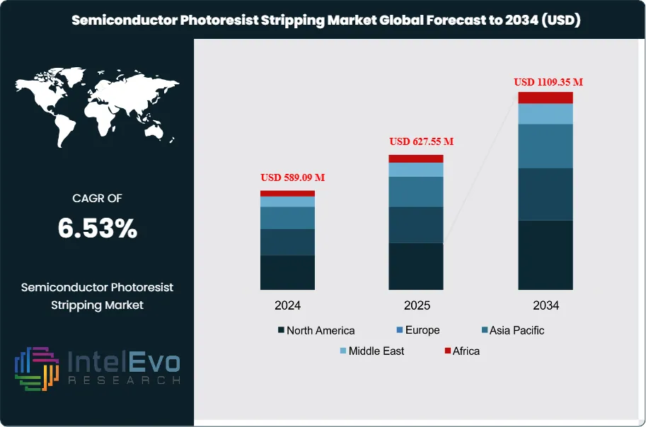
The Semiconductor Photoresist Stripping Market size is expected to be worth around USD 1109.35 Million by 2034, from USD 589.09 Million in 2024, growing at a CAGR of 6.53% during the forecast period from 2024 to 2034. The semiconductor photoresist stripping market is a critical component of the semiconductor manufacturing process. Photoresist stripping involves removing photoresist layers applied during lithography to create intricate patterns on silicon wafers.
This step is vital to ensure clean, defect-free surfaces for subsequent fabrication stages and is integral to producing high-quality integrated circuits (ICs). As semiconductor devices continually downscale in size and complexity, the demand for advanced photoresist stripping solutions grows, driven by the need for precision, efficiency, and environmental compliance.
Several factors influence the growth and evolution of the photoresist stripping market. One major factor is the rapid miniaturization of semiconductor devices. As chip manufacturers push for smaller feature sizes and higher transistor densities, the stripping process must become more selective and less damaging to delicate wafer surfaces. Advanced chemical formulations and plasma-based stripping techniques are increasingly favored to meet these stringent requirements. Additionally, the escalating adoption of emerging semiconductor applications, such as 5G communications, artificial intelligence (AI), and automotive electronics, further fuels market demand. Another significant market driver is the rising emphasis on eco-friendly manufacturing. Stricter environmental regulations worldwide are prompting semiconductor fabs to adopt greener, more sustainable photoresist stripping technologies which reduce hazardous waste and energy consumption without compromising stripping performance or yield.
Geographically, the semiconductor photoresist stripping market is strongly influenced by regional manufacturing hubs. The Asia-Pacific region dominates, accounting for almost half of the market revenue. This leadership is due to major semiconductor production centers in China, South Korea, Taiwan, and Japan, supported by substantial capital investments in fabs and aggressive policy initiatives like China’s “Made in China 2025.” North America—especially the United States—maintains a considerable share thanks to its technological expertise, robust innovation ecosystem, and presence of leading equipment and chemical suppliers. Europe also contributes to the market, driven by a focus on environmental regulations and ongoing investments in advanced manufacturing technologies.
The COVID-19 pandemic had a notable impact on the photoresist stripping market. Early in the crisis, semiconductor supply chains experienced disruptions from factory shutdowns, logistics restrictions, and material shortages, slowing production and investment in new stripping technologies. However, the pandemic also accelerated digital transformation trends and demand for electronic devices, creating a surge in chip consumption. This led to a rapid market recovery and intensified efforts toward automation and more resilient supply chains. The push for sustainability and efficiency in fabs also gained momentum as companies adapted to the new normal.
Regional conflicts and trade tensions between major economic players—most prominently between the United States and China—have introduced complex challenges for the semiconductor photoresist stripping market. Tariffs on semiconductor materials and equipment have increased operational costs and created uncertainties in sourcing critical chemicals and tools. Export controls on cutting-edge semiconductor technologies restrict technology flow and collaboration, forcing countries to localize parts of their supply chains. These geopolitical frictions contribute to market fragmentation, impact pricing strategies, and influence investment decisions, driving some manufacturers to diversify or onshore their fabrication capabilities to mitigate risk.
Nevertheless, international trade agreements continue to play a crucial role in shaping the global market landscape. Multilateral trade pacts such as the Regional Comprehensive Economic Partnership (RCEP) in Asia enhance trade and supply chain integration among member countries. The United States-Mexico-Canada Agreement (USMCA) facilitates semiconductor equipment movement and supports North American supply chains. Additionally, ongoing negotiations for technology cooperation and regulatory harmonization between regions help reduce tariff barriers and foster the development and distribution of advanced photoresist stripping technologies. These agreements support more stable and collaborative market growth despite geopolitical uncertainties.
Key Takeaways
Market Growth: The Semiconductor Photoresist Stripping Market is expected to reach USD 1109.35 Million by 2034, propelled by technology advances, shifts in regional manufacturing power, and evolving global trade dynamics.
Product Type Dominance: Positive photoresist stripper leads the market due to wider applicability and superior performance in standard processes.
Application Dominance: Integrated circuit manufacturing dominates the market, driven by continuous demand for advanced chip fabrication.
Technology Dominance: Wet stripping holds larger market share currently, owing to established infrastructure and cost-effectiveness.
End User Dominance: Foundries represent the fastest-growing segment, primarily due to increased fabless semiconductor design adoption.
Drivers: Key drivers accelerating growth include increasing complexity in semiconductor designs and rising demand for miniaturization, which boost market expansion through advanced fabrication requirements.
Restraints: Growth is hindered by high cost of advanced stripping technologies and stringent environmental regulations, which create challenges such as increased operational expenses and compliance requirements.
Opportunities: The market is poised for expansion due to opportunities like development of eco-friendly stripping solutions and adoption of advanced packaging technologies, which enable sustainable manufacturing and enhanced device performance.
Trends: Emerging trends including plasma-based dry stripping and automation in manufacturing are reshaping the market by improving precision and reducing environmental impact.
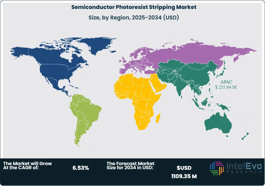
Regional Analysis: Asia-Pacific leads owing to concentrated semiconductor manufacturing and government support. North America and Europe show high promise due to technological innovation and sustainability focus.
Product Type Analysis:
The positive photoresist stripper segment maintains market leadership through its superior versatility and performance characteristics. This dominance stems from the segment's ability to handle diverse photoresist formulations used in modern semiconductor manufacturing. The positive stripping process offers advantages in processing speed and pattern resolution, critical factors as device geometries continue shrinking. Environmental considerations are driving development of aqueous-based positive strippers, aligning with sustainability trends while maintaining performance standards. The segment benefits from established supply chains and manufacturing expertise, creating barriers for alternative technologies. Market maturity in this segment provides stability but also intensifies competition on cost and performance optimization.
Application-Based Analysis:
Integrated Circuit Manufacturing Leads With over 65% Market Share In Semiconductor Photoresist Stripping Market. Integrated circuit manufacturing represents the cornerstone application driving market demand, benefiting from continuous expansion in consumer electronics, automotive semiconductors, and emerging technologies. This segment's leadership reflects the central role of photoresist stripping in IC fabrication processes, where precision and yield optimization directly impact profitability. The complexity of modern IC designs necessitates advanced stripping solutions capable of handling multiple photoresist layers and intricate pattern geometries. Wafer-level packaging applications, while smaller in current market share, demonstrate strong growth potential as advanced packaging techniques gain adoption. The IC manufacturing segment drives technological innovation through demanding requirements for selectivity, uniformity, and process control.
Technology-Based Analysis:
Wet stripping technology maintains market leadership through its proven reliability and cost-effectiveness in high-volume manufacturing environments. The established infrastructure supporting wet stripping processes provides significant competitive advantages, including mature process knowledge and optimized equipment designs. However, environmental regulations and sustainability concerns are gradually shifting preference toward dry stripping methods. Plasma-based dry stripping offers superior precision and reduced chemical waste, making it attractive for advanced node manufacturing. The technology transition reflects broader industry trends toward environmentally sustainable manufacturing practices while meeting increasingly stringent performance requirements for next-generation semiconductor devices.
End-User Analysis:
The foundry segment demonstrates the strongest growth momentum, driven by the continued expansion of fabless semiconductor business models and specialized manufacturing requirements. Foundries benefit from economies of scale and process specialization, enabling optimization of photoresist stripping operations across diverse customer requirements. IDMs maintain significant market presence through integrated manufacturing strategies, though many are transitioning toward hybrid models incorporating foundry partnerships. The competitive dynamics in this segment reflect broader semiconductor industry consolidation and specialization trends, with leading foundries investing heavily in advanced process capabilities to maintain technological leadership and customer relationships.
Regional Analysis
Asia-Pacific Leads With over 40% Market Share In Semiconductor Photoresist Stripping Market. Asia-Pacific maintains its position as the dominant regional market, driven by the concentration of major semiconductor manufacturing facilities in Taiwan, South Korea, and China. The region's leadership stems from substantial government investments in semiconductor infrastructure, favorable manufacturing costs, and proximity to major electronics markets. Taiwan's TSMC and South Korea's Samsung represent anchor customers driving significant demand for advanced photoresist stripping solutions. China's aggressive semiconductor development initiatives are creating new growth opportunities, though geopolitical considerations influence market dynamics.
North America holds approximately 30% market share, benefiting from technological innovation leadership and the presence of major equipment suppliers. The region's strength lies in R&D capabilities and early adoption of advanced manufacturing technologies. Environmental regulations in North America are driving development of sustainable stripping solutions, creating opportunities for companies focused on eco-friendly alternatives. Europe commands around 25% market share, with strong emphasis on environmental sustainability and regulatory compliance influencing technology adoption patterns. The region's focus on automotive semiconductors and industrial applications creates specialized demand for customized stripping solutions.
Product Type (Positive Photoresist Stripper, Negative Photoresist Stripper), (Application, Integrated Circuit Manufacturing, Wafer Level Packaging), Technology (Wet Stripping, Dry Stripping), End User (Foundries, IDMs (Integrated Device Manufacturers), Other Facilities)
Research Methodology
Primary Research- 100 Interviews of Stakeholders
Secondary Research
Desk Research
Regional scope
North America (United States, Canada, Mexico)
Latin America (Brazil, Argentina, Columbia)
East Asia And Pacific (China, Japan, South Korea, Australia, Cambodia, Fiji, Indonesia)
Sea And South Asia (India, Singapore, Thailand, Taiwan, Malaysia)
Eastern Europe (Poland, Russia, Czech Republic, Romania)
Western Europe (Germany, U.K., France, Spain, Itlay)
Middle East & Africa (GCC Countries, Egypt, Nigeria, South Africa, Israel)
Competitive Landscape
Applied Materials, Lam Research, Merck KGaA, Advanced Energy Industries, Brewer Science, EV Group, Screen Holdings Co. Ltd., Nordson Corp.
Customization Scope
Customization for segments, region/country-level will be provided. Moreover, additional customization can be done based on the requirements.
Pricing and Purchase Options
Avail customized purchase options to meet your exact research needs. We have three licenses to opt for: Single User License, Multi-User License (Up to 5 Users), Corporate Use License (Unlimited User and Printable PDF).
TABLE OF CONTENTS
1. EXECUTIVE SUMMARY
1.1. MARKET SNAPSHOT
1.2. KEY FINDINGS & INSIGHTS
1.3. ANALYST RECOMMENDATIONS
1.4. FUTURE OUTLOOK
2. RESEARCH METHODOLOGY
2.1. MARKET DEFINITION & SCOPE
2.2. RESEARCH OBJECTIVES: PRIMARY & SECONDARY DATA SOURCES
2.3. DATA COLLECTION SOURCES
2.3.1. COVERAGE OF 100+ PRIMARY RESEARCH/CONSULTATION CALLS WITH INDUSTRY STAKEHOLDERS
FIGURE 17 NORTH AMERICA SEMICONDUCTOR PHOTORESIST STRIPPING CURRENT AND FUTURE TYPE ANALYSIS, 2025–2034, (USD MILLION)
FIGURE 18 NORTH AMERICA SEMICONDUCTOR PHOTORESIST STRIPPING CURRENT AND FUTURE END USER ANALYSIS, 2025–2034, (USD MILLION)
FIGURE 19 MARKET SHARE BY COUNTRY
FIGURE 20 LATIN AMERICA SEMICONDUCTOR PHOTORESIST STRIPPING CURRENT AND FUTURE TYPE ANALYSIS, 2025–2034, (USD MILLION)
FIGURE 21 LATIN AMERICA SEMICONDUCTOR PHOTORESIST STRIPPING CURRENT AND FUTURE END USER ANALYSIS, 2025–2034, (USD MILLION)
FIGURE 22 MARKET SHARE BY COUNTRY
FIGURE 23 EASTERN EUROPE SEMICONDUCTOR PHOTORESIST STRIPPING CURRENT AND FUTURE TYPE ANALYSIS, 2025–2034, (USD MILLION)
FIGURE 24 EASTERN EUROPE SEMICONDUCTOR PHOTORESIST STRIPPING CURRENT AND FUTURE END USER ANALYSIS, 2025–2034, (USD MILLION)
FIGURE 25 MARKET SHARE BY COUNTRY
FIGURE 26 WESTERN EUROPE SEMICONDUCTOR PHOTORESIST STRIPPING CURRENT AND FUTURE TYPE ANALYSIS, 2025–2034, (USD MILLION)
FIGURE 27 WESTERN EUROPE SEMICONDUCTOR PHOTORESIST STRIPPING CURRENT AND FUTURE END USER ANALYSIS, 2025–2034, (USD MILLION)
FIGURE 28 MARKET SHARE BY COUNTRY
FIGURE 29 EAST ASIA AND PACIFIC SEMICONDUCTOR PHOTORESIST STRIPPING CURRENT AND FUTURE TYPE ANALYSIS, 2025–2034, (USD MILLION)
FIGURE 30 EAST ASIA AND PACIFIC SEMICONDUCTOR PHOTORESIST STRIPPING CURRENT AND FUTURE END USER ANALYSIS, 2025–2034, (USD MILLION)
FIGURE 31 MARKET SHARE BY COUNTRY
FIGURE 32 SEA AND SOUTH ASIA SEMICONDUCTOR PHOTORESIST STRIPPING CURRENT AND FUTURE TYPE ANALYSIS, 2025–2034, (USD MILLION)
FIGURE 33 SEA AND SOUTH ASIA SEMICONDUCTOR PHOTORESIST STRIPPING CURRENT AND FUTURE END USER ANALYSIS, 2025–2034, (USD MILLION)
FIGURE 34 MARKET SHARE BY COUNTRY
FIGURE 35 MIDDLE EAST AND AFRICA SEMICONDUCTOR PHOTORESIST STRIPPING CURRENT AND FUTURE TYPE ANALYSIS, 2025–2034, (USD MILLION)
FIGURE 36 MIDDLE EAST AND AFRICA SEMICONDUCTOR PHOTORESIST STRIPPING CURRENT AND FUTURE END USER ANALYSIS, 2025–2034, (USD MILLION)
FIGURE 37 NORTH AMERICA SEMICONDUCTOR PHOTORESIST STRIPPING CURRENT AND FUTURE MARKET VOLUME SHARE REGIONAL ANALYSIS, 2025–2034, (USD MILLION)
FIGURE 38 U.S. SEMICONDUCTOR PHOTORESIST STRIPPING CURRENT AND FUTURE TYPE ANALYSIS, 2025–2034, (USD MILLION)
FIGURE 39 U.S. SEMICONDUCTOR PHOTORESIST STRIPPING CURRENT AND FUTURE END USER ANALYSIS, 2025–2034, (USD MILLION)
FIGURE 40 CANADA SEMICONDUCTOR PHOTORESIST STRIPPING CURRENT AND FUTURE TYPE ANALYSIS, 2025–2034, (USD MILLION)
FIGURE 41 CANADA SEMICONDUCTOR PHOTORESIST STRIPPING CURRENT AND FUTURE END USER ANALYSIS, 2025–2034, (USD MILLION)
FIGURE 42 LATIN AMERICA SEMICONDUCTOR PHOTORESIST STRIPPING CURRENT AND FUTURE MARKET VOLUME SHARE REGIONAL ANALYSIS, 2025–2034, (USD MILLION)
FIGURE 43 MEXICO SEMICONDUCTOR PHOTORESIST STRIPPING CURRENT AND FUTURE TYPE ANALYSIS, 2025–2034, (USD MILLION)
FIGURE 44 MEXICO SEMICONDUCTOR PHOTORESIST STRIPPING CURRENT AND FUTURE END USER ANALYSIS, 2025–2034, (USD MILLION)
FIGURE 45 BRAZIL SEMICONDUCTOR PHOTORESIST STRIPPING CURRENT AND FUTURE TYPE ANALYSIS, 2025–2034, (USD MILLION)
FIGURE 46 BRAZIL SEMICONDUCTOR PHOTORESIST STRIPPING CURRENT AND FUTURE END USER ANALYSIS, 2025–2034, (USD MILLION)
FIGURE 47 ARGENTINA SEMICONDUCTOR PHOTORESIST STRIPPING CURRENT AND FUTURE TYPE ANALYSIS, 2025–2034, (USD MILLION)
FIGURE 48 ARGENTINA SEMICONDUCTOR PHOTORESIST STRIPPING CURRENT AND FUTURE END USER ANALYSIS, 2025–2034, (USD MILLION)
FIGURE 49 COLUMBIA SEMICONDUCTOR PHOTORESIST STRIPPING CURRENT AND FUTURE TYPE ANALYSIS, 2025–2034, (USD MILLION)
FIGURE 50 COLUMBIA SEMICONDUCTOR PHOTORESIST STRIPPING CURRENT AND FUTURE END USER ANALYSIS, 2025–2034, (USD MILLION)
FIGURE 51 REST OF LATIN AMERICA SEMICONDUCTOR PHOTORESIST STRIPPING CURRENT AND FUTURE TYPE ANALYSIS, 2025–2034, (USD MILLION)
FIGURE 52 REST OF LATIN AMERICA SEMICONDUCTOR PHOTORESIST STRIPPING CURRENT AND FUTURE END USER ANALYSIS, 2025–2034, (USD MILLION)
FIGURE 53 EASTERN EUROPE SEMICONDUCTOR PHOTORESIST STRIPPING CURRENT AND FUTURE MARKET VOLUME SHARE REGIONAL ANALYSIS, 2025–2034, (USD MILLION)
FIGURE 54 POLAND SEMICONDUCTOR PHOTORESIST STRIPPING CURRENT AND FUTURE TYPE ANALYSIS, 2025–2034, (USD MILLION)
FIGURE 55 POLAND SEMICONDUCTOR PHOTORESIST STRIPPING CURRENT AND FUTURE END USER ANALYSIS, 2025–2034, (USD MILLION)
FIGURE 56 RUSSIA SEMICONDUCTOR PHOTORESIST STRIPPING CURRENT AND FUTURE TYPE ANALYSIS, 2025–2034, (USD MILLION)
FIGURE 57 RUSSIA SEMICONDUCTOR PHOTORESIST STRIPPING CURRENT AND FUTURE END USER ANALYSIS, 2025–2034, (USD MILLION)
FIGURE 58 CZECH REPUBLIC SEMICONDUCTOR PHOTORESIST STRIPPING CURRENT AND FUTURE TYPE ANALYSIS, 2025–2034, (USD MILLION)
FIGURE 59 CZECH REPUBLIC SEMICONDUCTOR PHOTORESIST STRIPPING CURRENT AND FUTURE END USER ANALYSIS, 2025–2034, (USD MILLION)
FIGURE 60 ROMANIA SEMICONDUCTOR PHOTORESIST STRIPPING CURRENT AND FUTURE TYPE ANALYSIS, 2025–2034, (USD MILLION)
FIGURE 61 ROMANIA SEMICONDUCTOR PHOTORESIST STRIPPING CURRENT AND FUTURE END USER ANALYSIS, 2025–2034, (USD MILLION)
FIGURE 62 REST OF EASTERN EUROPE SEMICONDUCTOR PHOTORESIST STRIPPING CURRENT AND FUTURE TYPE ANALYSIS, 2025–2034, (USD MILLION)
FIGURE 63 REST OF EASTERN EUROPE SEMICONDUCTOR PHOTORESIST STRIPPING CURRENT AND FUTURE END USER ANALYSIS, 2025–2034, (USD MILLION)
FIGURE 64 WESTERN EUROPE SEMICONDUCTOR PHOTORESIST STRIPPING CURRENT AND FUTURE MARKET VOLUME SHARE REGIONAL ANALYSIS, 2025–2034, (USD MILLION)
FIGURE 65 GERMANY SEMICONDUCTOR PHOTORESIST STRIPPING CURRENT AND FUTURE TYPE ANALYSIS, 2025–2034, (USD MILLION)
FIGURE 66 GERMANY SEMICONDUCTOR PHOTORESIST STRIPPING CURRENT AND FUTURE END USER ANALYSIS, 2025–2034, (USD MILLION)
FIGURE 67 FRANCE SEMICONDUCTOR PHOTORESIST STRIPPING CURRENT AND FUTURE TYPE ANALYSIS, 2025–2034, (USD MILLION)
FIGURE 68 FRANCE SEMICONDUCTOR PHOTORESIST STRIPPING CURRENT AND FUTURE END USER ANALYSIS, 2025–2034, (USD MILLION)
FIGURE 69 UK SEMICONDUCTOR PHOTORESIST STRIPPING CURRENT AND FUTURE TYPE ANALYSIS, 2025–2034, (USD MILLION)
FIGURE 70 UK SEMICONDUCTOR PHOTORESIST STRIPPING CURRENT AND FUTURE END USER ANALYSIS, 2025–2034, (USD MILLION)
FIGURE 71 SPAIN SEMICONDUCTOR PHOTORESIST STRIPPING CURRENT AND FUTURE TYPE ANALYSIS, 2025–2034, (USD MILLION)
FIGURE 72 SPAIN SEMICONDUCTOR PHOTORESIST STRIPPING CURRENT AND FUTURE END USER ANALYSIS, 2025–2034, (USD MILLION)
FIGURE 73 ITALY SEMICONDUCTOR PHOTORESIST STRIPPING CURRENT AND FUTURE TYPE ANALYSIS, 2025–2034, (USD MILLION)
FIGURE 74 ITALY SEMICONDUCTOR PHOTORESIST STRIPPING CURRENT AND FUTURE END USER ANALYSIS, 2025–2034, (USD MILLION)
FIGURE 75 REST OF WESTERN EUROPE SEMICONDUCTOR PHOTORESIST STRIPPING CURRENT AND FUTURE TYPE ANALYSIS, 2025–2034, (USD MILLION)
FIGURE 76 REST OF WESTERN EUROPE SEMICONDUCTOR PHOTORESIST STRIPPING CURRENT AND FUTURE END USER ANALYSIS, 2025–2034, (USD MILLION)
FIGURE 77 EAST ASIA AND PACIFIC SEMICONDUCTOR PHOTORESIST STRIPPING CURRENT AND FUTURE MARKET VOLUME SHARE REGIONAL ANALYSIS, 2025–2034, (USD MILLION)
FIGURE 78 CHINA SEMICONDUCTOR PHOTORESIST STRIPPING CURRENT AND FUTURE TYPE ANALYSIS, 2025–2034, (USD MILLION)
FIGURE 79 CHINA SEMICONDUCTOR PHOTORESIST STRIPPING CURRENT AND FUTURE END USER ANALYSIS, 2025–2034, (USD MILLION)
FIGURE 80 JAPAN SEMICONDUCTOR PHOTORESIST STRIPPING CURRENT AND FUTURE TYPE ANALYSIS, 2025–2034, (USD MILLION)
FIGURE 81 JAPAN SEMICONDUCTOR PHOTORESIST STRIPPING CURRENT AND FUTURE END USER ANALYSIS, 2025–2034, (USD MILLION)
FIGURE 82 AUSTRALIA SEMICONDUCTOR PHOTORESIST STRIPPING CURRENT AND FUTURE TYPE ANALYSIS, 2025–2034, (USD MILLION)
FIGURE 83 AUSTRALIA SEMICONDUCTOR PHOTORESIST STRIPPING CURRENT AND FUTURE END USER ANALYSIS, 2025–2034, (USD MILLION)
FIGURE 84 CAMBODIA SEMICONDUCTOR PHOTORESIST STRIPPING CURRENT AND FUTURE TYPE ANALYSIS, 2025–2034, (USD MILLION)
FIGURE 85 CAMBODIA SEMICONDUCTOR PHOTORESIST STRIPPING CURRENT AND FUTURE END USER ANALYSIS, 2025–2034, (USD MILLION)
FIGURE 86 FIJI SEMICONDUCTOR PHOTORESIST STRIPPING CURRENT AND FUTURE TYPE ANALYSIS, 2025–2034, (USD MILLION)
FIGURE 87 FIJI SEMICONDUCTOR PHOTORESIST STRIPPING CURRENT AND FUTURE END USER ANALYSIS, 2025–2034, (USD MILLION)
FIGURE 88 INDONESIA SEMICONDUCTOR PHOTORESIST STRIPPING CURRENT AND FUTURE TYPE ANALYSIS, 2025–2034, (USD MILLION)
FIGURE 89 INDONESIA SEMICONDUCTOR PHOTORESIST STRIPPING CURRENT AND FUTURE END USER ANALYSIS, 2025–2034, (USD MILLION)
FIGURE 90 SOUTH KOREA SEMICONDUCTOR PHOTORESIST STRIPPING CURRENT AND FUTURE TYPE ANALYSIS, 2025–2034, (USD MILLION)
FIGURE 91 SOUTH KOREA SEMICONDUCTOR PHOTORESIST STRIPPING CURRENT AND FUTURE END USER ANALYSIS, 2025–2034, (USD MILLION)
FIGURE 92 REST OF EAST ASIA AND PACIFIC SEMICONDUCTOR PHOTORESIST STRIPPING CURRENT AND FUTURE TYPE ANALYSIS, 2025–2034, (USD MILLION)
FIGURE 93 REST OF EAST ASIA AND PACIFIC SEMICONDUCTOR PHOTORESIST STRIPPING CURRENT AND FUTURE END USER ANALYSIS, 2025–2034, (USD MILLION)
FIGURE 94 SEA AND SOUTH ASIA SEMICONDUCTOR PHOTORESIST STRIPPING CURRENT AND FUTURE MARKET VOLUME SHARE REGIONAL ANALYSIS, 2025–2034, (USD MILLION)
FIGURE 95 BANGLADESH SEMICONDUCTOR PHOTORESIST STRIPPING CURRENT AND FUTURE TYPE ANALYSIS, 2025–2034, (USD MILLION)
FIGURE 96 BANGLADESH SEMICONDUCTOR PHOTORESIST STRIPPING CURRENT AND FUTURE END USER ANALYSIS, 2025–2034, (USD MILLION)
FIGURE 97 NEW ZEALAND SEMICONDUCTOR PHOTORESIST STRIPPING CURRENT AND FUTURE TYPE ANALYSIS, 2025–2034, (USD MILLION)
FIGURE 98 NEW ZEALAND SEMICONDUCTOR PHOTORESIST STRIPPING CURRENT AND FUTURE END USER ANALYSIS, 2025–2034, (USD MILLION)
FIGURE 99 INDIA SEMICONDUCTOR PHOTORESIST STRIPPING CURRENT AND FUTURE TYPE ANALYSIS, 2025–2034, (USD MILLION)
FIGURE 100 INDIA SEMICONDUCTOR PHOTORESIST STRIPPING CURRENT AND FUTURE END USER ANALYSIS, 2025–2034, (USD MILLION)
FIGURE 101 SINGAPORE SEMICONDUCTOR PHOTORESIST STRIPPING CURRENT AND FUTURE TYPE ANALYSIS, 2025–2034, (USD MILLION)
FIGURE 102 SINGAPORE SEMICONDUCTOR PHOTORESIST STRIPPING CURRENT AND FUTURE END USER ANALYSIS, 2025–2034, (USD MILLION)
FIGURE 103 THAILAND SEMICONDUCTOR PHOTORESIST STRIPPING CURRENT AND FUTURE TYPE ANALYSIS, 2025–2034, (USD MILLION)
FIGURE 104 THAILAND SEMICONDUCTOR PHOTORESIST STRIPPING CURRENT AND FUTURE END USER ANALYSIS, 2025–2034, (USD MILLION)
FIGURE 105 TAIWAN SEMICONDUCTOR PHOTORESIST STRIPPING CURRENT AND FUTURE TYPE ANALYSIS, 2025–2034, (USD MILLION)
FIGURE 106 TAIWAN SEMICONDUCTOR PHOTORESIST STRIPPING CURRENT AND FUTURE END USER ANALYSIS, 2025–2034, (USD MILLION)
FIGURE 107 MALAYSIA SEMICONDUCTOR PHOTORESIST STRIPPING CURRENT AND FUTURE TYPE ANALYSIS, 2025–2034, (USD MILLION)
FIGURE 108 MALAYSIA SEMICONDUCTOR PHOTORESIST STRIPPING CURRENT AND FUTURE END USER ANALYSIS, 2025–2034, (USD MILLION)
FIGURE 109 REST OF SEA AND SOUTH ASIA SEMICONDUCTOR PHOTORESIST STRIPPING CURRENT AND FUTURE TYPE ANALYSIS, 2025–2034, (USD MILLION)
FIGURE 110 REST OF SEA AND SOUTH ASIA SEMICONDUCTOR PHOTORESIST STRIPPING CURRENT AND FUTURE END USER ANALYSIS, 2025–2034, (USD MILLION)
FIGURE 111 MIDDLE EAST AND AFRICA SEMICONDUCTOR PHOTORESIST STRIPPING CURRENT AND FUTURE MARKET VOLUME SHARE REGIONAL ANALYSIS, 2025–2034, (USD MILLION)
FIGURE 112 GCC COUNTRIES SEMICONDUCTOR PHOTORESIST STRIPPING CURRENT AND FUTURE TYPE ANALYSIS, 2025–2034, (USD MILLION)
FIGURE 113 GCC COUNTRIES SEMICONDUCTOR PHOTORESIST STRIPPING CURRENT AND FUTURE END USER ANALYSIS, 2025–2034, (USD MILLION)
FIGURE 114 SAUDI ARABIA SEMICONDUCTOR PHOTORESIST STRIPPING CURRENT AND FUTURE TYPE ANALYSIS, 2025–2034, (USD MILLION)
FIGURE 115 SAUDI ARABIA SEMICONDUCTOR PHOTORESIST STRIPPING CURRENT AND FUTURE END USER ANALYSIS, 2025–2034, (USD MILLION)
FIGURE 116 UAE SEMICONDUCTOR PHOTORESIST STRIPPING CURRENT AND FUTURE TYPE ANALYSIS, 2025–2034, (USD MILLION)
FIGURE 117 UAE SEMICONDUCTOR PHOTORESIST STRIPPING CURRENT AND FUTURE END USER ANALYSIS, 2025–2034, (USD MILLION)
FIGURE 118 BAHRAIN SEMICONDUCTOR PHOTORESIST STRIPPING CURRENT AND FUTURE TYPE ANALYSIS, 2025–2034, (USD MILLION)
FIGURE 119 BAHRAIN SEMICONDUCTOR PHOTORESIST STRIPPING CURRENT AND FUTURE END USER ANALYSIS, 2025–2034, (USD MILLION)
FIGURE 120 KUWAIT SEMICONDUCTOR PHOTORESIST STRIPPING CURRENT AND FUTURE TYPE ANALYSIS, 2025–2034, (USD MILLION)
FIGURE 121 KUWAIT SEMICONDUCTOR PHOTORESIST STRIPPING CURRENT AND FUTURE END USER ANALYSIS, 2025–2034, (USD MILLION)
FIGURE 122 OMAN SEMICONDUCTOR PHOTORESIST STRIPPING CURRENT AND FUTURE TYPE ANALYSIS, 2025–2034, (USD MILLION)
FIGURE 123 OMAN SEMICONDUCTOR PHOTORESIST STRIPPING CURRENT AND FUTURE END USER ANALYSIS, 2025–2034, (USD MILLION)
FIGURE 124 QATAR SEMICONDUCTOR PHOTORESIST STRIPPING CURRENT AND FUTURE TYPE ANALYSIS, 2025–2034, (USD MILLION)
FIGURE 125 QATAR SEMICONDUCTOR PHOTORESIST STRIPPING CURRENT AND FUTURE END USER ANALYSIS, 2025–2034, (USD MILLION)
FIGURE 126 EGYPT SEMICONDUCTOR PHOTORESIST STRIPPING CURRENT AND FUTURE TYPE ANALYSIS, 2025–2034, (USD MILLION)
FIGURE 127 EGYPT SEMICONDUCTOR PHOTORESIST STRIPPING CURRENT AND FUTURE END USER ANALYSIS, 2025–2034, (USD MILLION)
FIGURE 128 NIGERIA SEMICONDUCTOR PHOTORESIST STRIPPING CURRENT AND FUTURE TYPE ANALYSIS, 2025–2034, (USD MILLION)
FIGURE 129 NIGERIA SEMICONDUCTOR PHOTORESIST STRIPPING CURRENT AND FUTURE END USER ANALYSIS, 2025–2034, (USD MILLION)
FIGURE 130 SOUTH AFRICA SEMICONDUCTOR PHOTORESIST STRIPPING CURRENT AND FUTURE TYPE ANALYSIS, 2025–2034, (USD MILLION)
FIGURE 131 SOUTH AFRICA SEMICONDUCTOR PHOTORESIST STRIPPING CURRENT AND FUTURE END USER ANALYSIS, 2025–2034, (USD MILLION)
FIGURE 132 ISRAEL SEMICONDUCTOR PHOTORESIST STRIPPING CURRENT AND FUTURE TYPE ANALYSIS, 2025–2034, (USD MILLION)
FIGURE 133 ISRAEL SEMICONDUCTOR PHOTORESIST STRIPPING CURRENT AND FUTURE END USER ANALYSIS, 2025–2034, (USD MILLION)
FIGURE 134 REST OF MEA SEMICONDUCTOR PHOTORESIST STRIPPING CURRENT AND FUTURE TYPE ANALYSIS, 2025–2034, (USD MILLION)
FIGURE 135 REST OF MEA SEMICONDUCTOR PHOTORESIST STRIPPING CURRENT AND FUTURE END USER ANALYSIS, 2025–2034, (USD MILLION)
FIGURE 136 U. S. MARKET SHARE ANALYSIS BY TYPE (2024)
FIGURE 137 U. S. MARKET SHARE ANALYSIS BY END USER (2024)
FIGURE 138 CANADA MARKET SHARE ANALYSIS BY TYPE (2024)
FIGURE 139 CANADA MARKET SHARE ANALYSIS BY END USER (2024)
FIGURE 140 MEXICO MARKET SHARE ANALYSIS BY TYPE (2024)
FIGURE 141 MEXICO MARKET SHARE ANALYSIS BY END USER (2024)
FIGURE 142 CHINA MARKET SHARE ANALYSIS BY TYPE (2024)
FIGURE 143 CHINA MARKET SHARE ANALYSIS BY END USER (2024)
FIGURE 144 JAPAN MARKET SHARE ANALYSIS BY TYPE (2024)
FIGURE 145 JAPAN MARKET SHARE ANALYSIS BY END USER (2024)
FIGURE 146 INDIA MARKET SHARE ANALYSIS BY TYPE (2024)
FIGURE 147 INDIA MARKET SHARE ANALYSIS BY END USER (2024)
FIGURE 148 SOUTH KOREA MARKET SHARE ANALYSIS BY TYPE (2024)
FIGURE 149 SOUTH KOREA MARKET SHARE ANALYSIS BY END USER (2024)
FIGURE 150 SAUDI ARABIA MARKET SHARE ANALYSIS BY TYPE (2024)
FIGURE 151 SAUDI ARABIA MARKET SHARE ANALYSIS BY END USER (2024)
FIGURE 152 UAE MARKET SHARE ANALYSIS BY TYPE (2024)
FIGURE 153 UAE MARKET SHARE ANALYSIS BY END USER (2024)
FIGURE 154 EGYPT MARKET SHARE ANALYSIS BY TYPE (2024)
FIGURE 155 EGYPT MARKET SHARE ANALYSIS BY END USER (2024)
FIGURE 156 NIGERIA MARKET SHARE ANALYSIS BY TYPE (2024)
FIGURE 157 NIGERIA MARKET SHARE ANALYSIS BY END USER (2024)
FIGURE 158 SOUTH AFRICA MARKET SHARE ANALYSIS BY TYPE (2024)
FIGURE 159 SOUTH AFRICA MARKET SHARE ANALYSIS BY END USER (2024)
FIGURE 160 GERMANY MARKET SHARE ANALYSIS BY TYPE (2024)
FIGURE 161 GERMANY MARKET SHARE ANALYSIS BY END USER (2024)
FIGURE 162 FRANCE MARKET SHARE ANALYSIS BY TYPE (2024)
FIGURE 163 FRANCE MARKET SHARE ANALYSIS BY END USER (2024)
FIGURE 164 UK MARKET SHARE ANALYSIS BY TYPE (2024)
FIGURE 165 UK MARKET SHARE ANALYSIS BY END USER (2024)
FIGURE 166 SPAIN MARKET SHARE ANALYSIS BY TYPE (2024)
FIGURE 167 SPAIN MARKET SHARE ANALYSIS BY END USER (2024)
FIGURE 168 ITALY MARKET SHARE ANALYSIS BY TYPE (2024)
FIGURE 169 ITALY MARKET SHARE ANALYSIS BY END USER (2024)
FIGURE 170 BRAZIL MARKET SHARE ANALYSIS BY TYPE (2024)
FIGURE 171 BRAZIL MARKET SHARE ANALYSIS BY END USER (2024)
FIGURE 172 ARGENTINA MARKET SHARE ANALYSIS BY TYPE (2024)
FIGURE 173 ARGENTINA MARKET SHARE ANALYSIS BY END USER (2024)
FIGURE 174 COLUMBIA MARKET SHARE ANALYSIS BY TYPE (2024)
FIGURE 175 COLUMBIA MARKET SHARE ANALYSIS BY END USER (2024)
FIGURE 176 GLOBAL SEMICONDUCTOR PHOTORESIST STRIPPING CURRENT AND FUTURE MARKET KEY COUNTRY LEVEL ANALYSIS, 2024–2034, (USD MILLION)
FIGURE 177 FINANCIAL OVERVIEW:
Key Players Analysis
Applied Materials: Applied Materials maintains its position as a market leader through comprehensive portfolio coverage spanning both wet and dry photoresist stripping solutions, leveraging decades of semiconductor equipment expertise and global service capabilities. The company's technological leadership in plasma-based stripping systems positions it advantageously for the industry transition toward dry processing methods. Strategic investments in artificial intelligence and process optimization technologies enable differentiated product offerings that address customer requirements for improved yield and reduced operational costs. Applied Materials' extensive installed base provides recurring revenue opportunities through consumables, spare parts, and upgrade services, creating sustainable competitive advantages. The company's global manufacturing and service infrastructure supports rapid technology deployment and customer support across all major semiconductor markets, reinforcing its market leadership position.
Lam Research: Lam Research has established strong market presence through focused innovation in plasma-based etch and clean technologies, with photoresist stripping representing a natural extension of core competencies in semiconductor surface preparation. The company's expertise in plasma chemistry and process control translates directly to advanced stripping applications requiring precise selectivity and damage-free processing. Strategic partnerships with leading photoresist suppliers enable co-optimization of stripping processes for new material systems, providing competitive differentiation through superior performance. Lam Research's commitment to sustainability through development of environmentally friendly processes aligns with industry trends toward green manufacturing practices. The company's strong financial position enables continued investment in R&D and strategic acquisitions to expand technology portfolio and market reach.
Merck KGaA: Merck KGaA leverages its extensive chemical expertise and materials science capabilities to develop innovative photoresist stripping formulations addressing evolving requirements for advanced semiconductor manufacturing. The company's integrated approach combining photoresist materials with compatible stripping chemicals provides system-level optimization opportunities that differentiate its offerings from equipment-focused competitors. Strategic investments in sustainable chemistry development position Merck advantageously for the industry transition toward environmentally friendly manufacturing practices. The company's global chemical manufacturing and distribution infrastructure enables efficient supply chain management and local customer support across all major semiconductor markets. Merck's strong intellectual property portfolio in specialty chemicals provides competitive protection and licensing revenue opportunities, supporting long-term market positioning and profitability.
Market Key Players
Applied Materials
Lam Research
Merck KGaA
Advanced Energy Industries
Brewer Science
EV Group
Screen Holdings Co. Ltd.
Nordson Corp.
Drivers
Increasing Complexity in Semiconductor Designs:
The relentless advancement of semiconductor technology drives fundamental changes in photoresist stripping requirements, as modern devices incorporate increasingly complex architectures with multiple photoresist layers, fine-pitch patterns, and diverse material compositions. Advanced node manufacturing at 7nm and below necessitates stripping solutions capable of handling extreme aspect ratios and maintaining critical dimension control throughout the process. Three-dimensional device structures, including FinFET and gate-all-around architectures, create unique challenges for photoresist removal in confined geometries. The proliferation of specialized semiconductor applications, from high-performance computing to automotive electronics, demands customized stripping solutions optimized for specific performance criteria. System-on-chip designs incorporating diverse functional blocks require stripping processes capable of handling multiple photoresist types within single manufacturing flows, driving demand for versatile and precise stripping technologies.
Rising Demand for Miniaturization:
The semiconductor industry's continuous push toward smaller device geometries creates increasingly stringent requirements for photoresist stripping precision and selectivity, as any process variation can significantly impact device performance and yield. Advanced packaging technologies, including chip-scale packages and wafer-level processing, require stripping solutions capable of maintaining structural integrity while achieving complete photoresist removal. The transition to extreme ultraviolet lithography introduces new photoresist chemistries requiring specialized stripping approaches to avoid damage to underlying materials. Mobile device requirements for thinner profiles and higher functionality density drive demand for advanced stripping techniques supporting ultra-thin wafer processing and through-silicon via fabrication. Internet of Things applications requiring miniaturized sensors and communication devices create new market segments with specific stripping requirements for MEMS and specialized device structures.
Restraints
High Cost of Advanced Stripping Technologies:
The development and implementation of next-generation photoresist stripping systems require substantial capital investments that can strain manufacturer resources and limit technology adoption, particularly among smaller fabrication facilities and emerging market players. Advanced dry stripping equipment incorporating plasma generation systems, sophisticated process control, and contamination management features command premium pricing that may not be justified for all manufacturing applications. Research and development costs for new stripping chemistries and processes require multi-year investment commitments with uncertain market acceptance, creating financial risks for equipment suppliers and chemical manufacturers. The need for specialized facilities, safety systems, and waste management infrastructure adds significant operational overhead costs that impact overall manufacturing economics. Training requirements for advanced stripping technologies create additional costs and implementation barriers, as specialized expertise may not be readily available in all geographic markets.
Stringent Environmental Regulations:
Global environmental regulations governing chemical waste disposal, air emissions, and worker safety create complex compliance requirements that increase operational costs and limit technology options for photoresist stripping applications. Restrictions on volatile organic compounds and hazardous air pollutants require expensive emission control systems and alternative chemistry development, impacting both equipment suppliers and end users. Waste treatment and disposal costs for spent stripping chemicals represent significant ongoing operational expenses, particularly for high-volume manufacturing facilities. Regulatory uncertainty regarding future environmental standards creates planning challenges for long-term technology investments and facility development. International variations in environmental regulations complicate global manufacturing strategies and technology standardization efforts, requiring customized solutions for different geographic markets.
Opportunities
Development of Eco-Friendly Stripping Solutions:
The growing emphasis on environmental sustainability creates significant market opportunities for companies developing green alternatives to traditional photoresist stripping chemicals and processes, addressing both regulatory requirements and corporate sustainability goals. Bio-based stripping formulations derived from renewable feedstocks offer potential for reduced environmental impact while maintaining performance standards required for semiconductor manufacturing. Closed-loop chemical recovery systems enable recycling of stripping solvents and reduction of waste streams, creating value propositions based on both environmental and economic benefits. Plasma-based dry stripping technologies offer inherent environmental advantages through elimination of liquid chemical waste and reduced emission potential, though requiring continued development for broader application coverage. Water-based stripping systems combined with advanced filtration and treatment technologies enable sustainable manufacturing practices while meeting performance requirements for advanced semiconductor devices.
Adoption of Advanced Packaging Technologies:
The semiconductor industry's transition toward advanced packaging architectures creates new market segments requiring specialized photoresist stripping solutions optimized for unique geometric and material constraints. Three-dimensional integrated circuits incorporating through-silicon vias and multiple die stacking require stripping processes capable of handling complex topographies and diverse material interfaces. System-in-package architectures combining different semiconductor technologies demand versatile stripping solutions accommodating varied photoresist types and process requirements within integrated manufacturing flows. Chiplet-based designs enabling modular semiconductor architectures create opportunities for customized stripping processes supporting heterogeneous integration approaches. Advanced thermal interface materials and electromagnetic shielding requirements in modern packages necessitate specialized stripping solutions compatible with novel material systems and processing constraints.
Trends
Plasma-Based Dry Stripping Adoption:
The semiconductor industry is experiencing accelerated adoption of plasma-based dry stripping technologies, driven by superior precision control and environmental advantages compared to traditional wet stripping methods. Advanced plasma systems incorporating multiple gas chemistries and sophisticated endpoint detection enable selective removal of photoresist layers while preserving underlying materials with minimal damage. Process monitoring and control capabilities in modern plasma stripping systems provide real-time feedback for optimization and yield improvement, addressing critical requirements for advanced node manufacturing. Integration of artificial intelligence and machine learning algorithms in plasma stripping equipment enables predictive maintenance and process optimization, reducing operational costs and improving manufacturing efficiency. The transition toward plasma stripping reflects broader industry trends toward dry processing methods that minimize chemical waste and environmental impact while meeting increasingly stringent performance requirements.
Automation and Smart Manufacturing Integration:
The implementation of Industry 4.0 principles in semiconductor manufacturing is driving integration of photoresist stripping operations into comprehensive automation and data analytics platforms, enabling optimized process control and predictive maintenance capabilities. Advanced sensor technologies and real-time monitoring systems provide continuous feedback on stripping process parameters, enabling immediate adjustments to maintain optimal performance and yield. Machine learning algorithms analyzing historical process data enable predictive optimization of stripping parameters for different device types and manufacturing conditions, reducing development time and improving consistency. Integration with manufacturing execution systems enables comprehensive tracking of stripping process performance and correlation with downstream device characteristics, supporting continuous improvement initiatives. Robotic material handling and automated equipment maintenance systems reduce manual intervention requirements and improve operational consistency, addressing labor shortage challenges and safety concerns in semiconductor manufacturing environments.
Recent Development
In February 2025: JSR Corporation is broadening its global efforts in the development and manufacturing of advanced photoresists by opening a new research and development center in Japan and building a semiconductor photoresist manufacturing facility in South Korea. Following its acquisition of Inpria Corporation in 2021, JSR has been advancing the commercialization of Metal Oxide Resist (MOR) technology for EUV lithography. The upcoming R&D center located in Japan’s Kanto region will strengthen collaboration with international clients and partners, while the Korean production plant, scheduled to start operations in 2026, will focus on the final manufacturing stages of MOR to support local market deployment. Through these initiatives, JSR aims to foster innovation in photoresist technology and assist customers in establishing commercial production globally.
In December 2024: High-purity photoresists play a crucial role in manufacturing chips for advanced production nodes. As China works toward achieving self-sufficiency in its semiconductor industry, it must focus on developing not only advanced chipmaking equipment but also high-purity photoresist materials. In 2024, China made significant progress in the development of photoresists, driven by government support and increasing demand from domestic semiconductor manufacturers.
Frequently Asked Questions
How big is the Semiconductor Photoresist Stripping Market?
The global Semiconductor Photoresist Stripping Market is projected to grow at a CAGR of 6.53%, rising from USD 589.09 Million in 2024 to USD 1109.35 Million by 2034.
Who are the major players in the Semiconductor Photoresist Stripping Market?
Applied Materials, Lam Research, Merck KGaA, Advanced Energy Industries, Brewer Science, EV Group, Screen Holdings Co. Ltd., Nordson Corp.
Which segments covered the Semiconductor Photoresist Stripping Market?
Product Type (Positive Photoresist Stripper, Negative Photoresist Stripper), (Application, Integrated Circuit Manufacturing, Wafer Level Packaging), Technology (Wet Stripping, Dry Stripping), End User (Foundries, IDMs (Integrated Device Manufacturers), Other Facilities)
How can this market research report help my business make strategic decisions?
Our market research reports provide actionable intelligence, including verified market size data, CAGR projections, competitive benchmarking, and segment-level opportunity analysis. These insights support strategic planning, investment decisions, product development, and market entry strategies for enterprises and startups alike.
How frequently is the data updated?
We continuously monitor industry developments and update our reports to reflect regulatory changes, technological advancements, and macroeconomic shifts. Updated editions ensure you receive the latest market intelligence.